I had already written extensively in February about the new board requirements and the more complex manufacturing process. And that’s exactly how it happens now, so I’ll go into it in more detail in a moment. But for many people, the actual state of production is certainly much more interesting. I also have exclusive information for this, because all major manufacturers are already running the so-called pilot production. Only with the BIOS (also for last tests) one is not quite finished, but at least almost. The current status today is RC2, so you’re close to the finish there as well.
Many board partners will not start with the reference board known as PG132, but with their own designs, even if usually with a few days offset. There is also a lot of talk about the coolrs, but I have to stick to imposed NDAs here. But it is being spread that, for example. Asus will come up with three 100 mm fans on the Strix models, which should bring the card length to well over 32 cm. As a reminder: the FE relies on two 110 mm propellers.
To prevent benchmark leaks, NVIDIA has also completely sealed off the evaluation drivers this time. I don’t even think Furmark, let alone Time Spy, is running anymore, but only NVPunish (a stress testing program) for the thermal tests. Therefore all benchmark results leaked so far should be treated with absolute caution. Also from a board partner’s point of view it is of course quite strange when you produce something you don’t even know how fast it will be in the end.
Nvidia relies on 12 layers and the backdrill method for amps
A nasty cost driver, also for the board partners, is the very complex circuit board. But from the GeForce RTX “3080” up, it definitely has to be 12 layers (5 cores), according to NVIDIA’s rules, which also apply to the board partners and their own boards. The 12-layer boards and the necessary backdrill (I’ll come back to that in a minute) cost a lot of money, but are essential for the use of GDDR6X and the new Base Design Kit. And so several times there were rumours of horrified sales managers and controllers who asked the technicians quite helplessly where the additional costs suddenly came from.
But back to the backdrill. This technology is not new, but it is much more complex and thus more expensive than the “normal” production of the previously known multi-layer boards (6 to 8 layers for the graphics cards) including simple vias and stubs, i.e. the unneeded remnants (extensions) of vias that can be found on any board with several layers. Let us therefore look at the section through a simple circuit board and the signal path. The blue line shows the original signal path via vias in the transition from one layer (one layer) to another. The red line shows that within the so-called stub (blunt, residual hole) an additional reflected signal can occur, which arrives at the next layer with a time delay as a “ghost”.
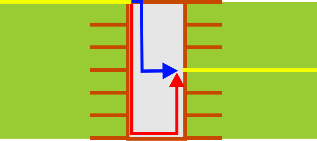
In the high-frequency range, such effects are of course the death of any signal integrity, because these stubs can lead not only to reflections but also to capacitance, inductance and impedance disturbances. These in turn are all errors that increase with increasing propagation speed/bit rate. In the worst case, a signal may even become unusable. However, since Nvidia uses the method called backdrill to remove these stubs (which is more expensive), it can be concluded that both the targeted frequencies and the targeted bit rates should increase significantly, which certainly justifies the conclusion of the probability of a significant performance increase.
Through the so-called backdrill process, i.e. a second step, these holes can now be drilled out and thus the stubs removed. In the end, this is even more efficient and easier to handle than using so-called blind holes, where you only drill as far as necessary for a through-hole plating or the use of “buried” holes inside the board, where you no longer see any through-hole plating on the outside. However, these two methods are once again much more complex and therefore more expensive. Backdrill it is, then:

This automatically results in a significantly lower bit error rate, avoids jitter and can reduce signal attenuation. This leads to a higher channel bandwidth and higher data rates. Which brings us back to the starting point of the consideration of performance enhancement. According to Samsung, there is currently no significantly faster GDDR6 available than the 16Gbps, so Nvidia’s change in manufacturing technology for the new boards must be viewed rather blanketly for all areas where signal integrity and bandwidth are important. So something really fast will be waiting for us, that’s for sure.
The possible package as graphic
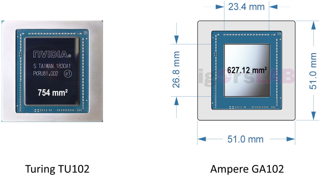
And now my small, highly speculative work of art from June comes into play, which is based on measurements that have been passed on and which corresponds quite well with my June projection at the time. It is also identical to what Komachi wrote on Twitter a month later. If the information is correct, the edge lengths of the chip would result in a chip area of 627.12 mm². The maximum number of shaders possible here is of course also related to their complexity and nobody can say how the ratio of CUDA to RT and especially Tensor cores will be.









Kommentieren