


Already in June Intel brought its 3. Gen Xeon Scalable CPU family, also known as the “Cooper Lake”, but still based on the 14nm architecture. Now some people in mainland China (where else?) have gotten their hands on the first QA (Qualified Sample) of Cooper Lake chips, which have an interesting design for the family of LGA 4189 CPUs based on the Cedar Island platform.
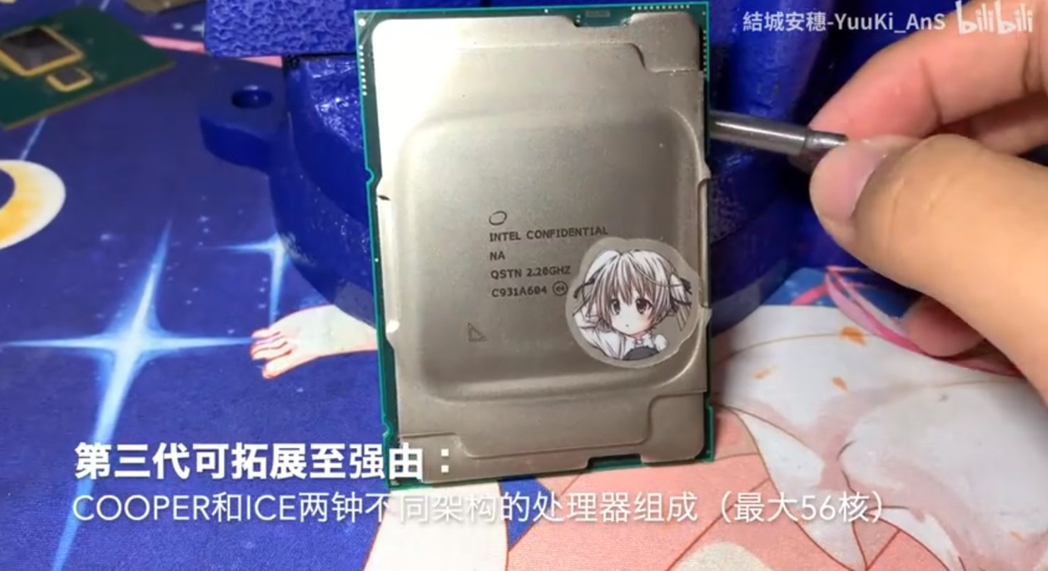
Through the Twitter account of Momomo_US a link was posted to the Bilibili video platform, where you can see a special Cooper Lake SP-QS of the Intel Xeon Gold 5320H. This CPU should have over 20 cores / 40 threads and be based on the 14nm++ node from Intel. It is to have a base clock of 2.2 GHz and be produced as early as 2019, around the beginning of August, one year before the official market launch in June 2020.
Cooper Lake
LGA 4189
QSTN 2.2GHZ (Xeon Gold 5320H ES)
Solder pic.twitter.com/Z6FeUY1Igx— 188号 (@momomo_us) July 26, 2020
However, the official specifications for the Xeon Gold 5320H mention a base clock of 2.4 GHz and a boost clock of 4.3 GHz. The difference in clock speeds is again due to the qualification, i.e. the build status / stepping of the chip itself, which is well before the official specifications for the Cooper Lake SP product line are defined. But the base clock is not the only change we see in this chip compared to its final form of sale.
A look at the IHS shows a striking similarity to the older Cooper Lake (CPX-4) version. The Intel Cooper Lake product line was originally developed for both Cedar Island and Whitley platforms (discontinued). It was actually expected to see up to 56 cores and 112 threads, but Intel will now probably only release the 10nm Ice Lake SP CPUs for the Whitley platform, which would also be a major update within the Xeon landscape since the introduction of Skylake-SP (2015).
Other, much higher quality images than these video screens of the Cooper Lake-SP QS-CPU are from the Twitter account Brutus (@brutuscat2).
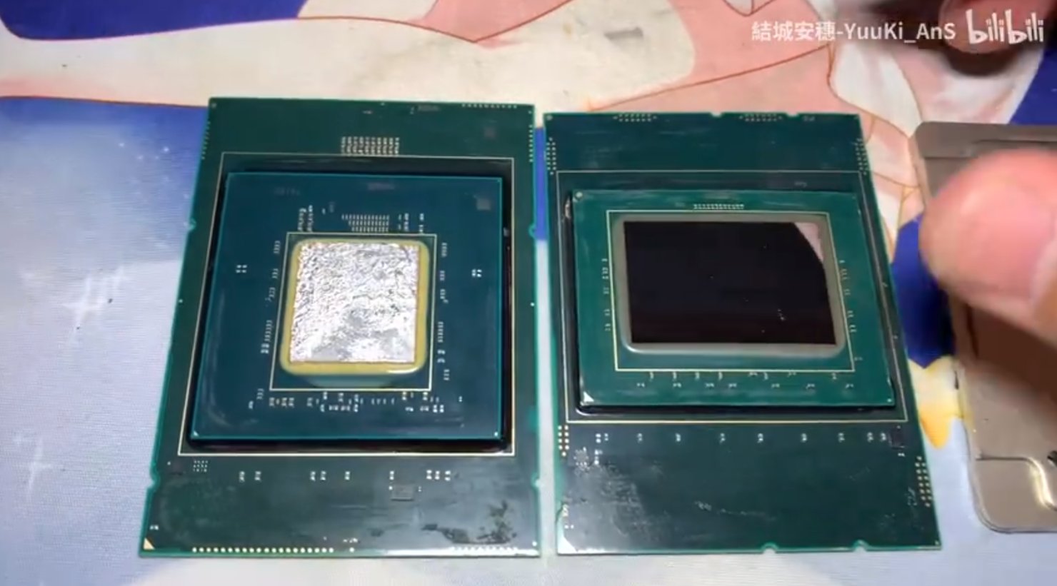
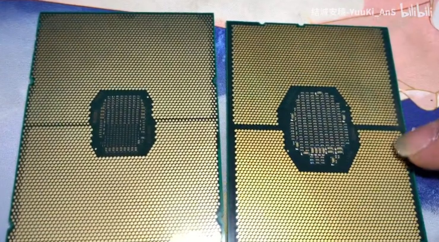
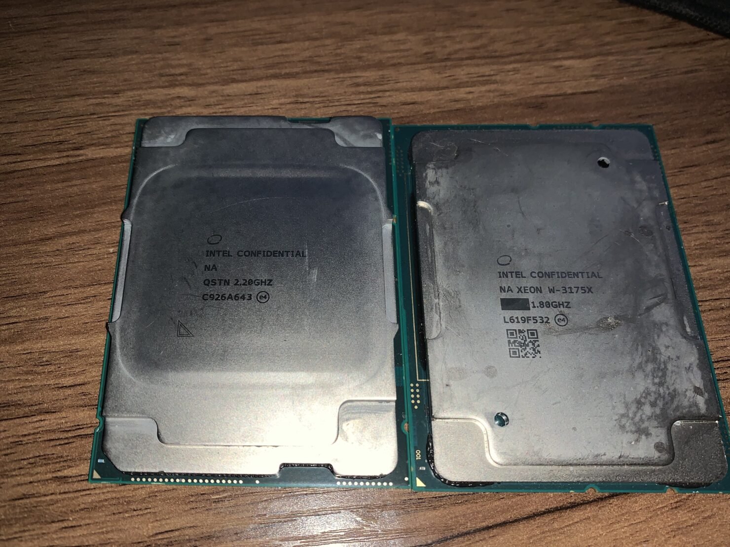
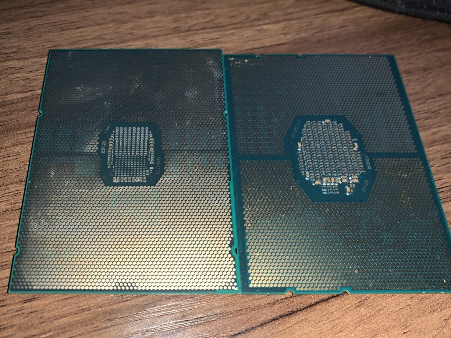
LGA 4189-4 (left, CPX-4) vs LGA 3647 (right, 3175X ES) pic.twitter.com/HPxCcRPSVj
— Brutus (@brutuscat2) July 26, 2020
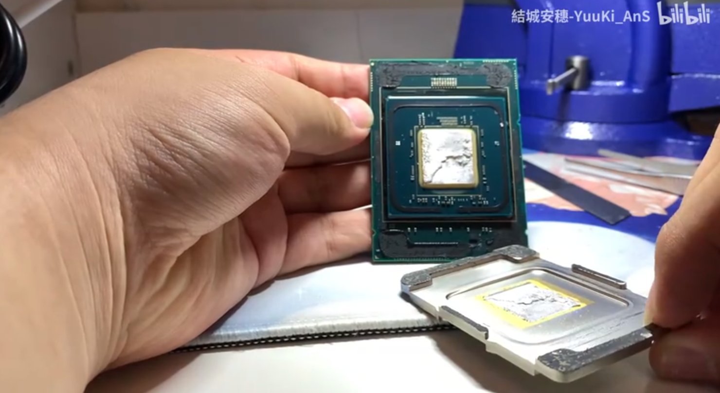
The chip uses a dual-package design, which is the usual design choice of Intel today. The silicon for this is located on a separate package interposer, which is located on the top of the motherboard. Next to a Xeon W-3175X, the Cooper Lake-SP looks much bigger and that’s ultimately the reason why it needs a larger socket (LGA 4189) to be able to run it compared to the Xeons of the last generation of Cascade Lake-SP (LGA 3647).
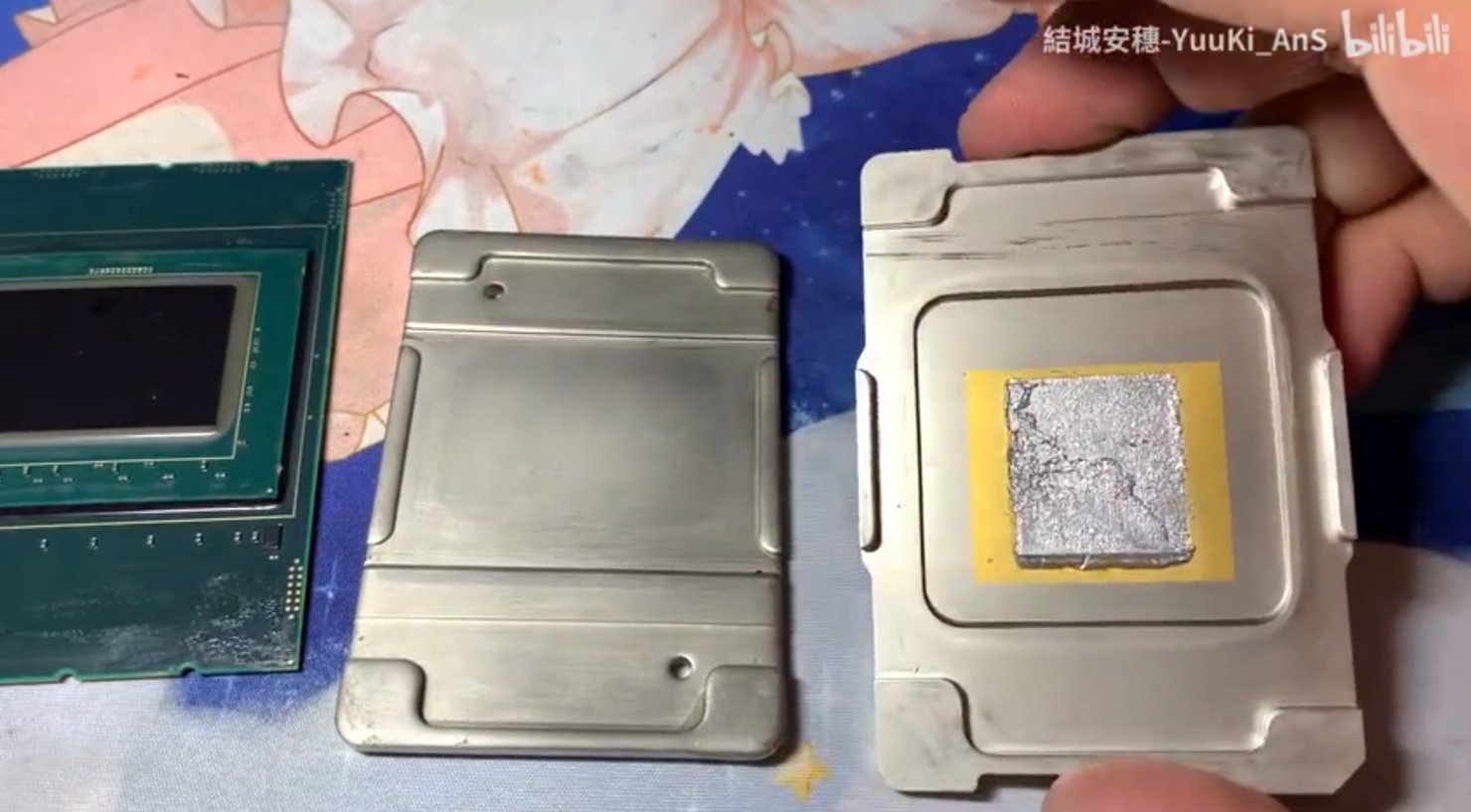
Other interesting details are the materials used under the IHS, which have a gold-plated surface and a design “soldered” with high-quality liquid metal heat-conducting paste. It is not possible to say with certainty whether the retail versions also have gold plated components like this QA, but considering that the competitor already does, one could assume that Cooper Lake-SP uses the same materials on the final chips.
Another interesting detail now revealed by this deal is the fact that the chip uses an HCC die (High Core Count) and not the XCC die (Extreme Core Count), which allows more than 18 cores. Such a HCC die normally only scales up to 18 cores, but here you see a HCC die that is even used for a chip with 20 cores and 40 threads. This is really remarkable, but further information is missing completely.
Source: twitter, wccftech


Kommentieren