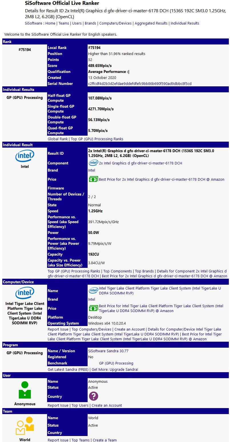
TumApisak has discovered something again, specifically a new entry in the database of Sisoft Sandra, and this is also promptly distributed as usual on Twitter. It seems that a multi-GPU setup consisting of two Intel Xe LPs with 1.25 GHz clock speed each was used and entered there before a run. But whether this is really a real dedicated mGPU package or the (not yet correctly detected) tiles of a Xe HP solution remains open.
According to Sisoft Sandra, it is a dual-GPU solution based on Xe LP cores with 96 EUs each. This in turn corresponds to a total number of 1536 cores, which were operated with a 1.25 GHz clock. This clock rate suggests that it is probably an engineering sample from Intel’s labs, since the final clock rates of a real dGPU are likely to be at least 1.5 GHz. The 4 .6 TFLOPS would certainly be good for a decent graphics card in the entry-level segment, as long as the price is right.
Overall, however, it seems that Intel is taking the MCM approach very seriously, in a similar way to AMD, and that such solutions, which were previously only intended for high-end applications, will become an integral part of the overall strategy for Intel’s GPUs. It would also come quite close to the handwriting and philosophy of Raja Koduri, who has been trying to realize exactly this vision for years. One can therefore assume that this was more a kind of validation platform for the Xe HP architecture, which is still to come, so in the end it could even have been a real Xe HP 2-Tiles-GPU, with Sisoft Sandra simply misreading the architecture.
I’ve reported on this several times, both about Intel’s Xe and the MCM approach that both AMD and Intel are taking. It remains to be seen what the final outcome will be, but on the other hand it already leaves a lot of room for speculation.


Kommentieren