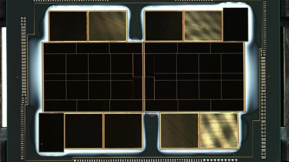
Intel had unveiled one of the world’s biggest chips not too long ago and the picture that emerges after all the releases so far is quite overwhelming. Intel’s Xe HPC 2-Tile (PVC) GPU uses a mix of Intel’s 7nm, Intel’s 10nm ESF and TSMC’s 7nm (or 5nm) process technology for this, which is brought together in Foveros 3D packaging. The Intel Xe HPC 2-Tile package shown by Intel’s chief architect Raja Koduri (which is pretty much the equivalent of the Ponte Vecchio GPU in its early stages) is certainly an absolute marvel in terms of the technology used. However, huge amounts of electrical energy are also converted into heat, but more on that in a moment.
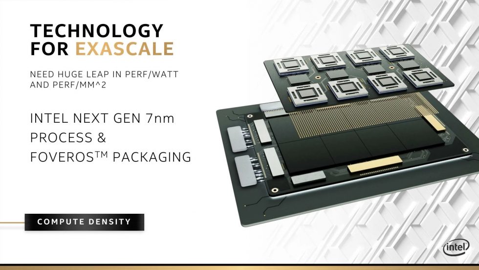
Let’s briefly recap what we already know. The graphic above shows EMIB in use together with Fovero’s 3D packaging. You can also see the promised mix-and-match philosophy with parts from TSMC and new features like Rambo Cache (thanks to Usman Pirzada for all the details, too). Since this package is based on Intel’s 3D-Foveros technology, a lot of things are still covered and hidden and as long as you don’t get a detailed 3D-diagram with the single layers, you can only guess the complexity of the package. So is the enormous power consumption.
But how do you cool such a monster?
To investigate this question, I got some more exclusive information. Ponte Vecchio is designed as an OAM module. The OCP Accelerator Module (OAM) specification defines an open hardware compute accelerator module form factor and its interconnects. Of course, the whole thing can only be cooled sensibly with water, because we are talking about up to 600 watts per module (or even a little more).
The exclusive construction drawing below illustrates once again the enormous size of the package and the exact dimensions of the mounting kit, from which one can also deduce the package itself.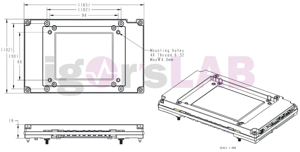
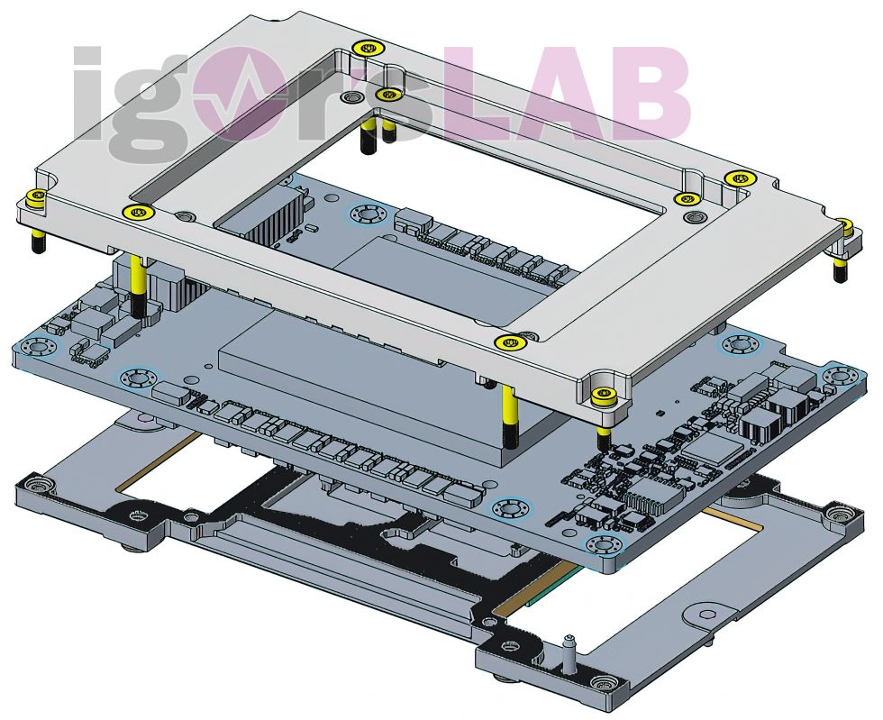
The next figure shows the composition of the bottom plate (bottom), the PCB of the OAM module (middle) and the cover (top plate, top). You can also clearly see the necessary leave-out areas for the active and passive components of the OAM and the cut-out for the cold plate on the GPU.
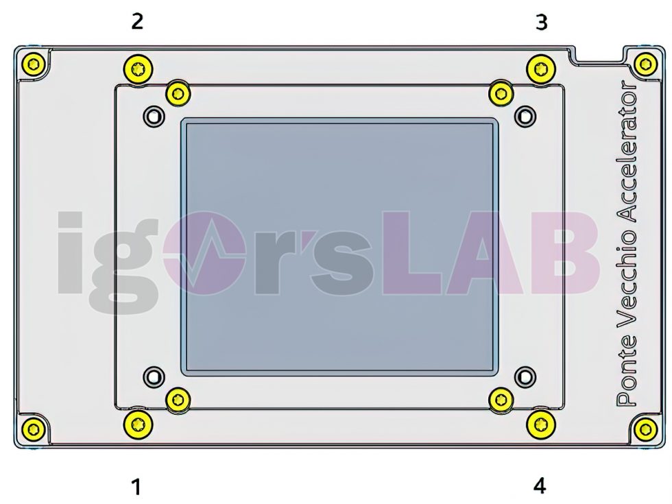
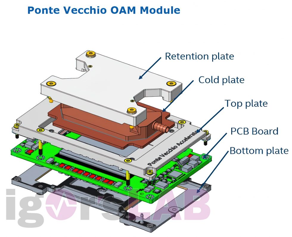
Finally, I now have the complete composition of such a unit including the Cold-Plate and the Retention-Plate as topping.
When exactly the whole thing will actually run remains to be seen. Here, Raja Koduri, as chief architect, is now under a bit of pressure to move and succeed. So let’s be surprised, the part with the cooling from the Intel documents looks at least very plausible.






3 Antworten
Kommentar
Lade neue Kommentare
Mitglied
Mitglied
Mitglied
Alle Kommentare lesen unter igor´sLAB Community →