


Terrible SoC voltages everywhere! AMD’s new horror! Say some YouTubers. But to learn more about this problem and understand why at first glance everything seems different than it actually is, we need to go back to the source, which is none other than SVI3. In this article today I will try to shed more light on this power interface used by AMD’s latest processors.
After I published the first article and especially the video, many users complained that I did not measure behind the CPU socket and that there could be a significant voltage drop on the PCB traces. Knowing that the corresponding traces are thick enough NOT to allow high voltage drops, and from the fact that the VRMs have current sense lines to adjust their output according to the load and voltage drops, I was not that concerned about it. Nevertheless, I took new measurements on the motherboard’s measurement pads and behind the CPU socket.
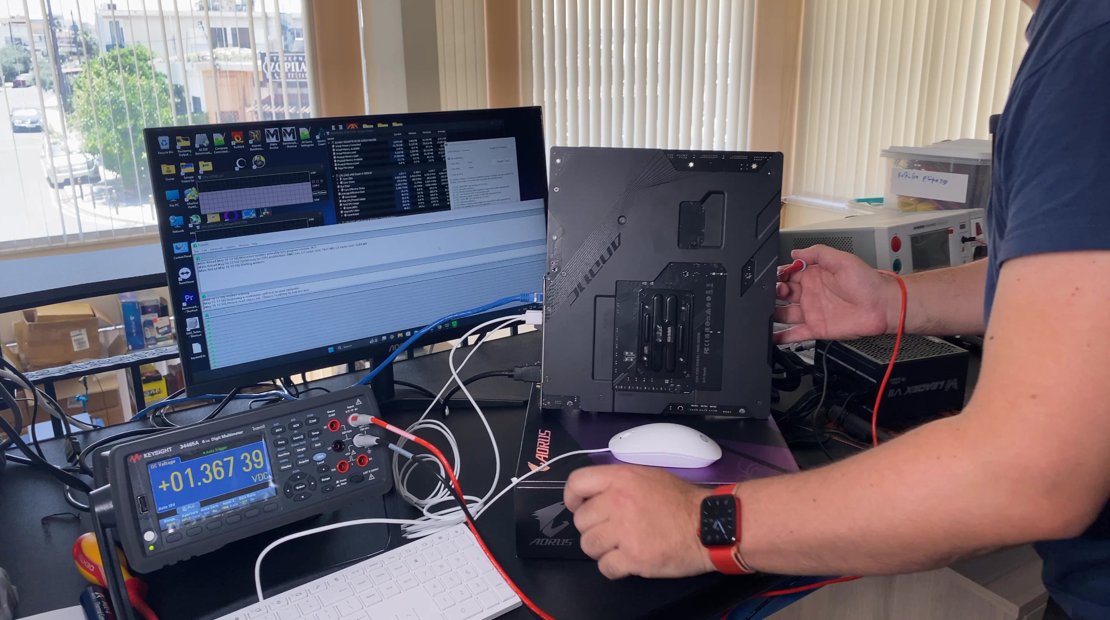
As you can see, the drop between the motherboard’s VRM output and the socket is only 0.01445V, with Prime95 running, which loads the CPU to the max. Now that we have that cleared up as well, let’s move on to the main article, which is about SVI3.
The Scalable Voltage Interface 3 (SVI3)
SVI3 is designed to provide faster and more precise control over the voltage required by the processor. It establishes a two-way communication protocol between the CPU and the motherboard’s voltage regulator modules (VRMs), allowing the CPU to control its current requirements alongside monitoring the power supply. There are some PWM controllers that are compatible with the SVI3 interface. The CPU has real-time information about the power and operating conditions of the mainboard’s VRMs. When the CPU does not need much power, it can turn off some VRMs to reduce power losses.
The CPU can enable or disable the power phases of the VRMs by sending the appropriate command to the power controller through the I2C bus. The AM5 socket has three different power rails that provide power to the CPU. One is shared between the CPU and the embedded graphics cores; the SoC rail is mainly for the I/O die (IOD), and the VDD rail is for the Infinity Fabric and other miscellaneous things.
There is almost no information about SVI3 from AMD. So I had to look for the older SVI2, on which SVI3 is based. Modern CPUs need to monitor dynamically and adjust the voltage rails that feed them accordingly. Since the CPU is generating the load, it is ideal to be able to control its power source. This could also be the case with power supplies. In fact, the ATX v3.0 and PCIe 5.0 standards use it through the 12VHPWR connector and its sinusoidal signals: CARD_PWR_STABLE and CARD_CBL_PRES# (Optional), but they are optional and I don’t see them implemented in the end.
But back to the topic at hand, the SVI2 and SVI3 are three-line interfaces with clock (SVC), data (SVD), and telemetry (SVT) lines. The SVI2 and SVI3 protocols are similar to the concept of the I²C bus, so the CPU as the master sends control packets over the SVC (clock) and SVD (data) lines to the VRM circuits of the mainboard.

For SVI2, the control packets consist of 3 bytes transmitted according to the SMBus send byte protocol: 1 byte to select the voltage range (core or SoC), followed by an acknowledgement bit (ACK), and then 2 bytes containing the voltage to be applied and other configuration parameters, each byte followed by an ACK bit. Because of the configuration coding, the voltage can be configured with a step size of 6.25 mV. The telemetry function (TFN) configuration bits can enable periodic voltage (and current) reports from the VR to the CPU via the SVC and SVT lines.
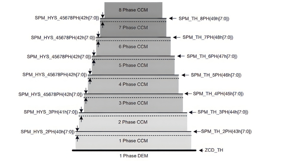
In SVI3, we have three rails, core, SoC, and VDD, so the first byte in the control packet must be used for three options instead of two in SVI2. The VRMs of the mainboard receive or send I2C signals through the I2C interface. The CPU sends various commands (read/write/reset registers, VID/address packets, change power state, and telemetry request) to the VRMs. There is a loop controller that controls the on/off sequence of the VRMs, handles protection functions, and controls the PWM operation of the VRMs.
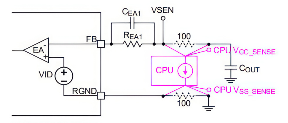
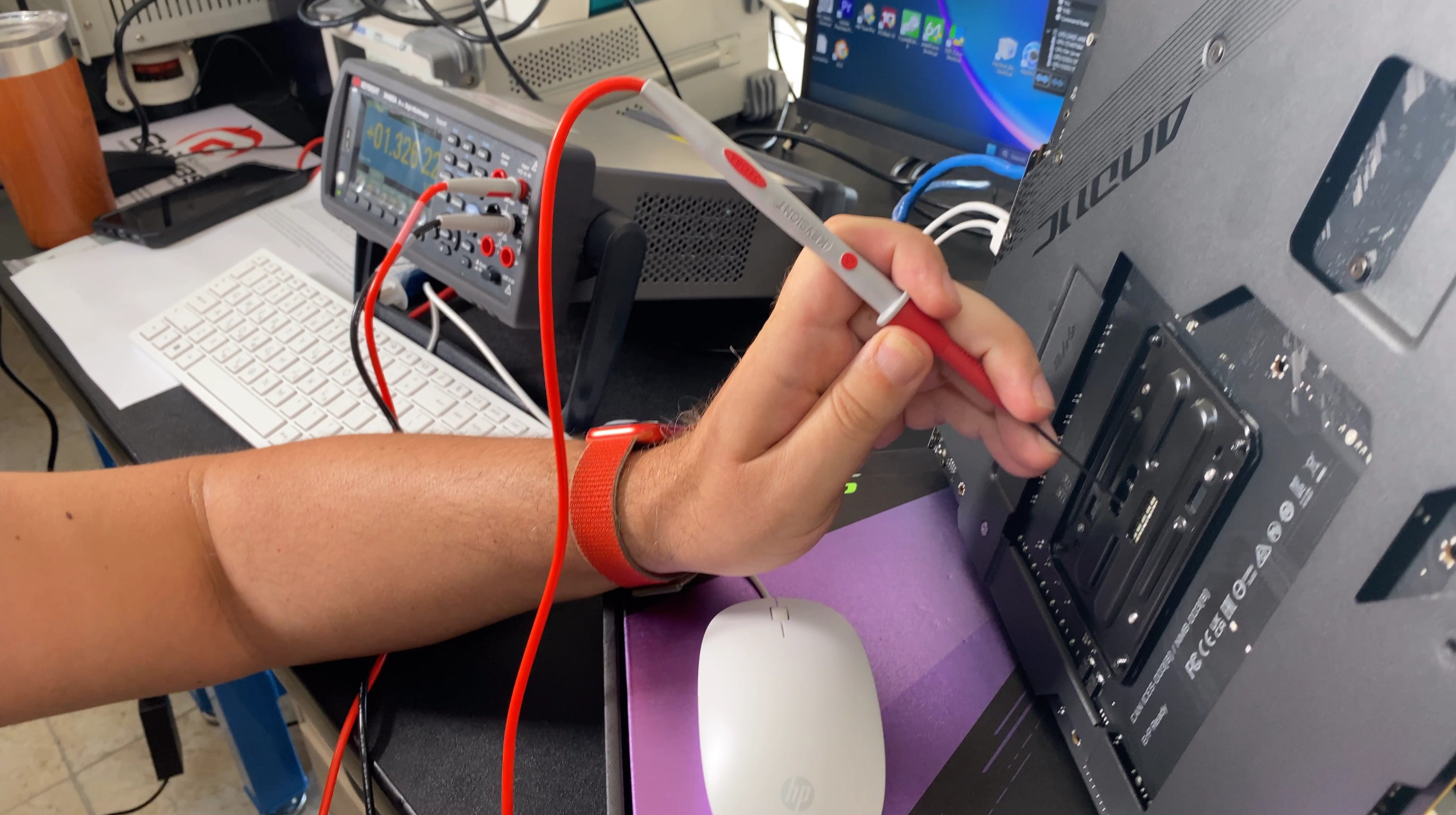
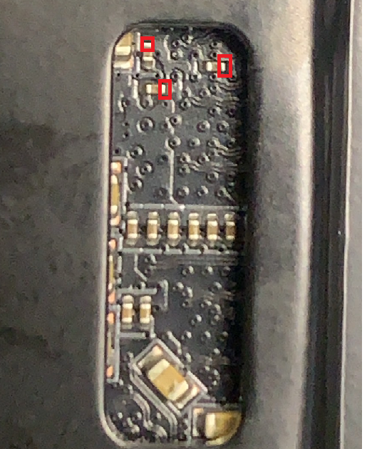
The CPU includes on die integrated sensor inputs, VCC_SENSE and VSS_SENSE. If no CPU is installed and manufacturers want to test the motherboard, pairs of 100Ω resistors are required to close the circuit and provide voltage feedback. VSEN and RGND must be routed as differential pairs from the VRM controller to the CPU socket without crossing any phase node, gate driver, VIN current delivery path, and high-speed signals. VSEN is ideal for accurate measurements without having to account for voltage drops.
Most importantly, there is a remote measurement line between the VRMs and the load (the CPU) to handle voltage drops along the PCB traces, the CPU’s internal current routers, and the socket contacts. So not only is there a voltage drop on the motherboard, but we also have a drop on the pins of the motherboard that are connected to the CPU and inside the CPU!
For telemetry information, the CPU takes data from the controller, which continuously monitors the output voltage of the VRMs, from the differential voltage sensor input (VSEN pin and RGND pin). Some power controllers average the data for higher accuracy to reduce measurement noise. The controller also collects information about the current output (Iout) and temperature to the CPU. So if the CPU detects that something is wrong, it can make the appropriate changes to the VRM operation using the data provided.
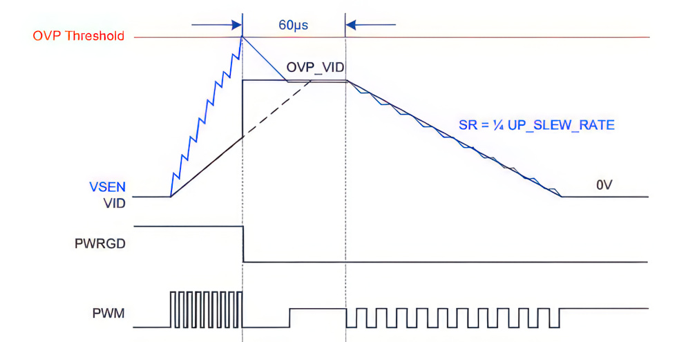
I would like to note that most of the protection functions are handled by the motherboard current controller, including overcurrent, overheat, undervoltage, and overvoltage protection. For example, when the overvoltage protection is triggered, the controller forces the low-voltage MOSFETs to turn on, so the high-voltage MOSFETs are turned off and the VRMs are disconnected from the input of the power supply (12V).
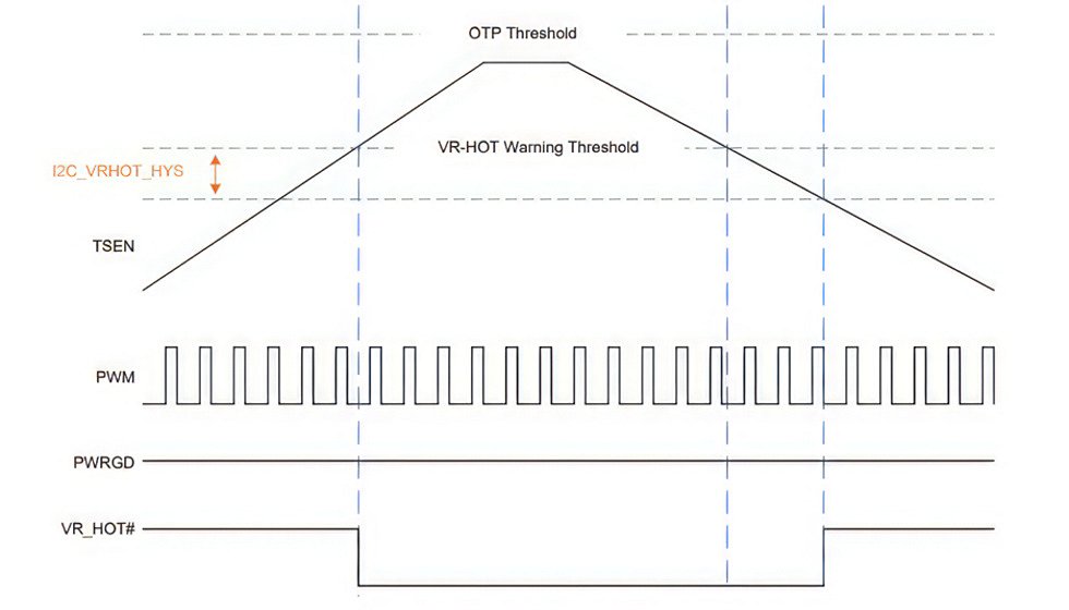
Regarding the overheat protection, when the controller receives an “overheat” signal, it transmits it to the CPU via the I2C bus, and it reduces the power consumption by reducing the CPU load. Therefore, the quality of VRMs is important for the speed of the CPU. If VRMs get hot quickly during overload, the CPU must reduce its load to let them cool down.
Conclusions and conclusion
From all this, we can come to the following conclusions:
- SVI3 allows the CPU to fully control the VRM phases of the motherboard.
- SVI3 can not only take measurements, but also provide all types of measurements, including of course all voltage levels fed to the corresponding circuits of the CPU.
- The only way to get voltage measurements inside the CPU is to use SVI3.
- We have no way of knowing if the measurements SVI3 provides inside the CPU are accurate because we cannot measure them externally.
- There is a voltage drop between the VRM output of the motherboard and the socket, which in my case, for the VSOC, under full load, is 0.01445V.
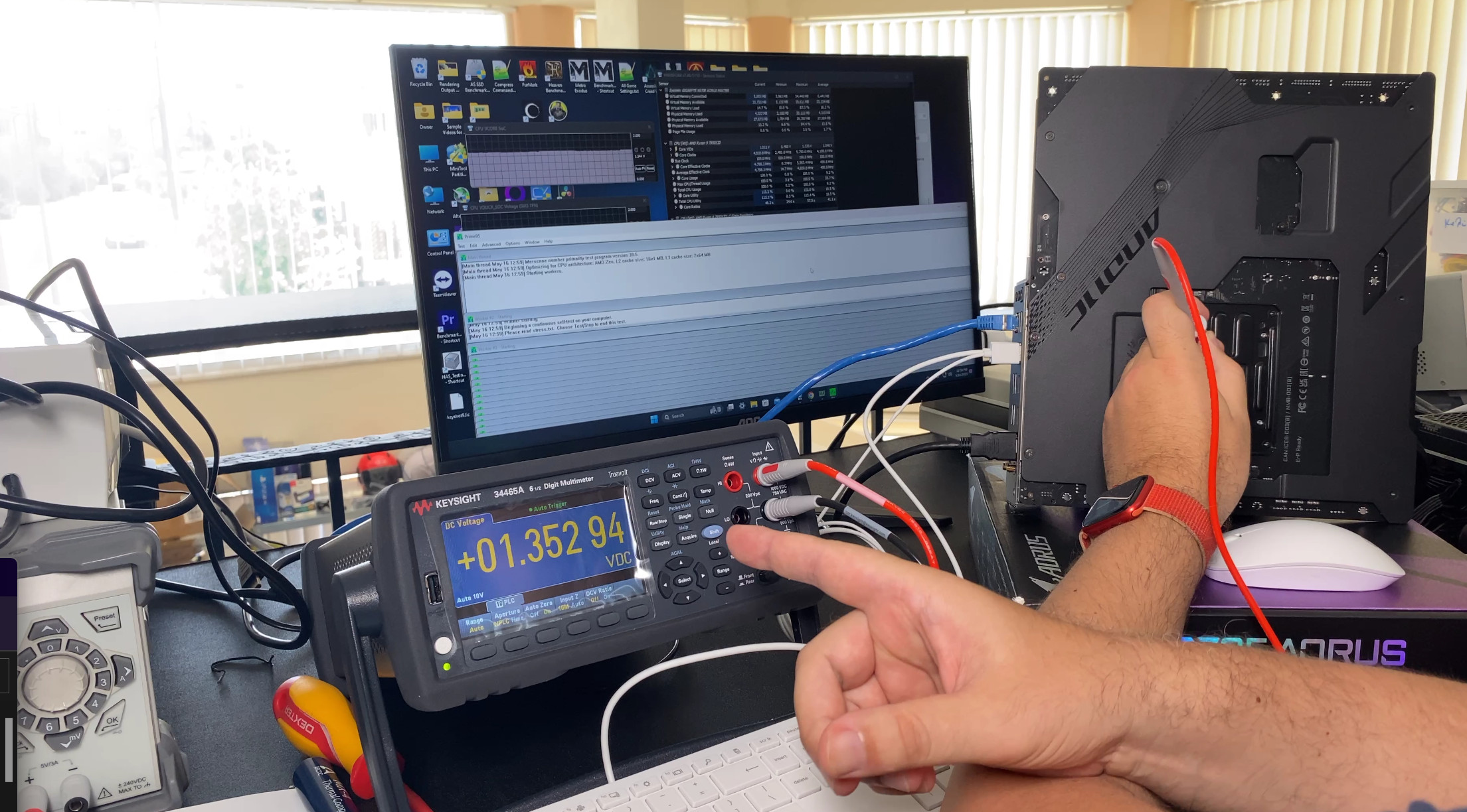
- There is a voltage drop between the socket’s power connection and what the CPU’s internal circuits receive, due to the connections through the motherboard’s pins and the power losses within the CPU’s internal power lines. In my case, I measured 1.35294V on the back of the socket, while the CPU VDDCR_SOC (SVI3 TFN) voltage was 1.295V as reported by HWinfo. This means that from the back of the socket to the corresponding circuit of the CPU, the voltage drop is 0.05794V, while if you take the motherboard VRM output as a starting point, the voltage drop is 0.07239V, which is significant.
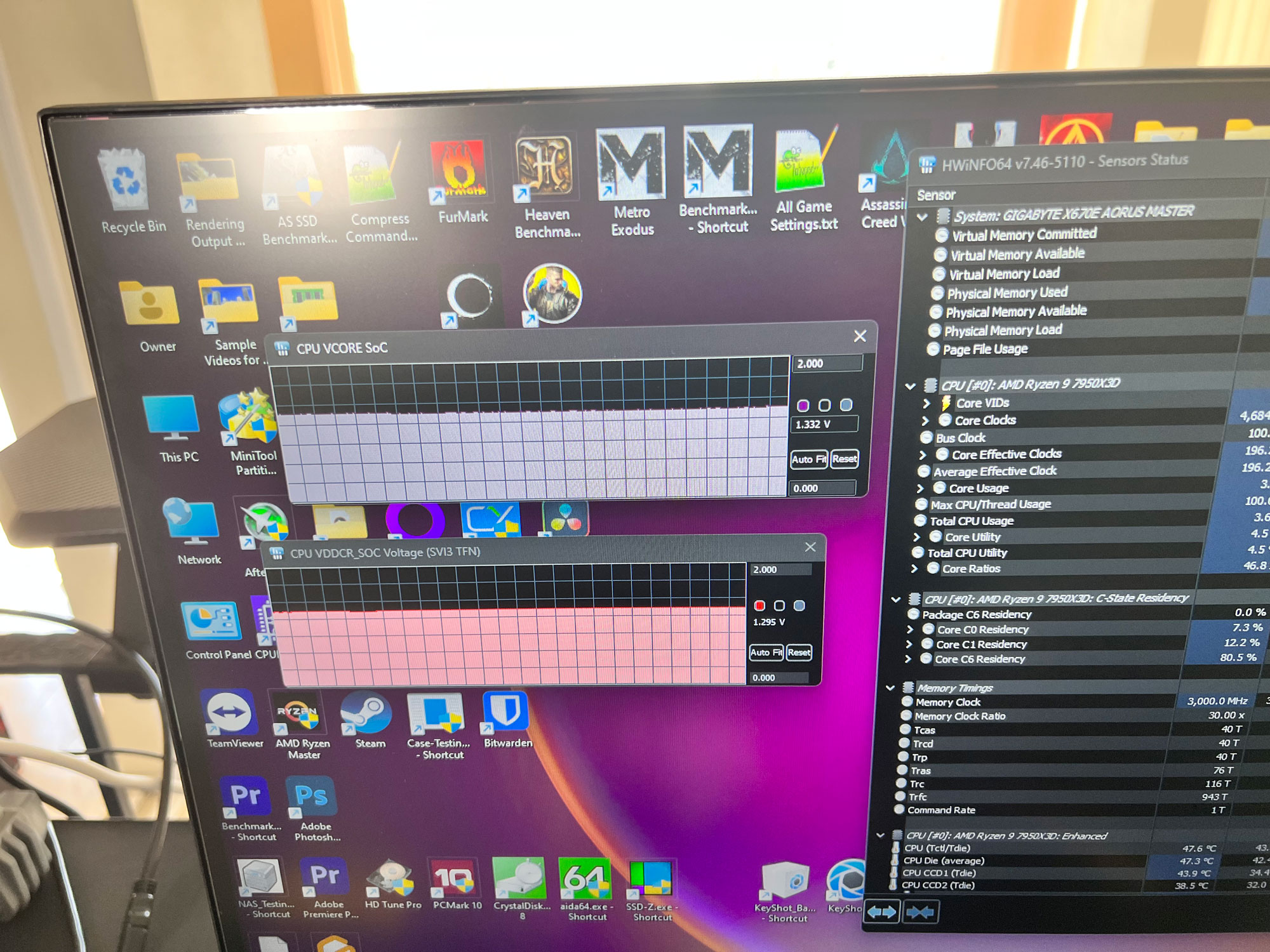
AMD has stated that anything above 1.30V VSOC is unsafe and should be avoided, but has not clarified at what point. At the motherboard VRMs, at the back of the sockets, or in the internal circuitry of the CPU? I talked to people from Gigabyte and they told me that they try to keep the VSOC voltage below 1.3V according to the information from SVI3, which means inside the CPU where we can’t make measurements by physical means, only by software. A lower VSOC SVI3 voltage than 1.30V, for example 1.25V, creates problems for RAM kits with EXPO profile enabled.
From all this, I can safely assume that if you check your motherboard CPU VDDCR_SOC voltage (SVI3 TFN) and find that it is below 1.30V (while running a stressful benchmark and EXPO is enabled), you can also be sure that everything always runs according to AMD’s specifications. For me, the problem is that I can’t take physical measurements of this voltage and I’m troubled by the significant voltage drop of 0.05794V between the CPU socket and the circuitry inside the CPU. But this is said to be even higher for Intel.
References and sources:
- Advanced Micro Devices, Inc. 2018. understanding power management and processor performance determinism. Retrieved 2023-05-17 from https://www.amd.com/system/files/documents/understanding-power-management.pdf
- Buhren, R., Jacob, H. N., Krachenfels, T., & Seifert, J. (2021). One Glitch to Rule Them All: Fault Injection Attacks Against AMD’s Secure Encrypted Virtualization. ArXiv. /abs/2108.04575
- Renesas Electronics Corporation. 2020. ISL62776 Multiphase PWM Regulator for AMD CPUs Using SVI2. Retrieved 2023-05-17 from https://www.renesas.com/us/en/document/dst/isl62776-datasheet
- Richtek Technology Corporation. 2023. Dual Channel PWM Controller with I2C Interface Control for AMD SVI3 CPU/GPU Core Power Supply. Retrieved 2023-05-17 from https://www.richtek.com/assets/product_file/RT3667BT/DS3667BT-00.pdf
My thanks go to the guest author, whose insights I am of course happy to share. If you want to know more about Aris, hwbusters.com (this article was also first published here) and Cybenetics i would like to recommend the respective homepages. You will find unique content based on real and independent measurements. I also recommend the new Powenetics V2 PMD or reading about the product:


164 Antworten
Kommentar
Lade neue Kommentare
Urgestein
Mitglied
Urgestein
1
Urgestein
Veteran
Veteran
1
1
Urgestein
Urgestein
1
Mitglied
1
Urgestein
Urgestein
Urgestein
Urgestein
Alle Kommentare lesen unter igor´sLAB Community →