


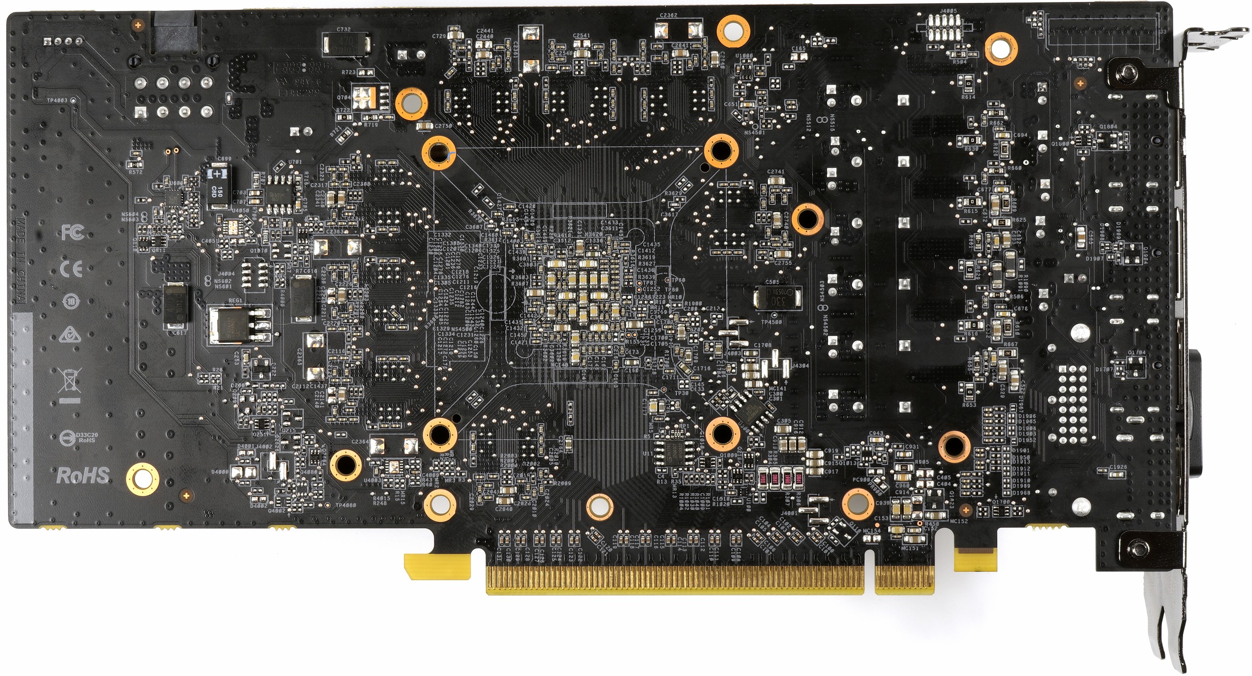
Power supply and layout
The board is a multi-layer design and is manufactured by Yu Fo Electronics Co Ltd in Taoyuan (Taiwan). Although it differs significantly from the old reference layout of the Radeon RX 480 at first glance, it is still very much in the same vein in many respects.
We now take a closer look at the board and at first glance immediately see the much-advertised six supply phases for the GPU. However, due to the existing 8-pin connection, there are less problems in assigning these phases to the individual rails (PCI-Express external, motherboard slot). We will, of course, measure the respective loads later. ASRock also relies on polymer capacitors at the critical points of VR, but in cup form.
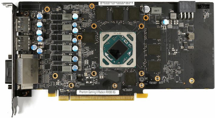
We don’t want to miss out on manual assembly, but you can already see that large components such as the coils were not used by machine. The soldering quality of the board is fine, the simple surface sealing of the back also.
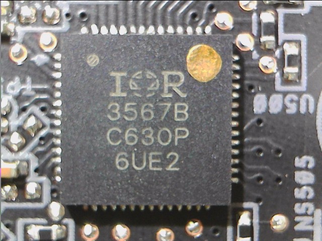
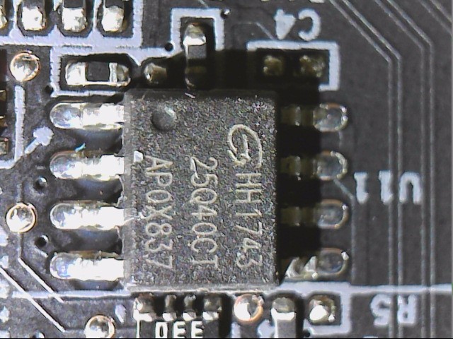
The IR3567B from International Rectifier is a good old acquaintance. This is a dual-loop digital multi-phase buck controller, i.e. a control chip for two separately operating voltage converter layouts (max. 6 + 2 phases). In our case, here it controls the six real phases for the GPU and another for memory.
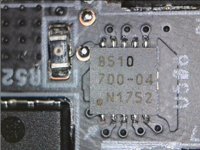
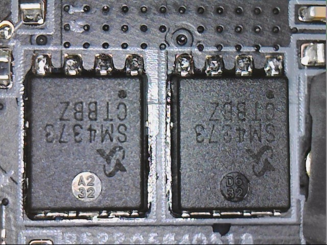
The CHL8510 used as an OEM product is the IR3537 and is one of the most widely used gate drivers for controlling high and low-side voltage converter circuits. ASRock uses it to control the six GPU phases.
 |
 |
The connection of the VRM is classically solved. Instead of relying on a highly integrated single chip (PowerStage), like some manufacturers, the implementation is carried out with individual components, which is of course also easier to cool in the end, since the heat density on such a large area is significantly lower. We will see later that this can work well.
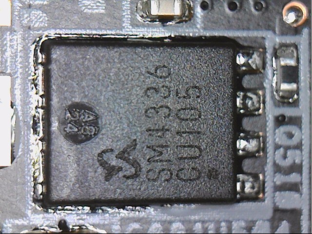
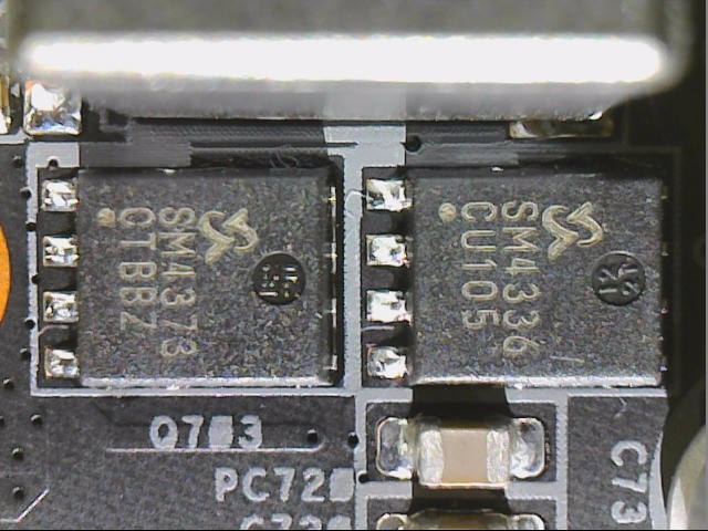
It is equipped with a single SM4336 and the low-side with two SM4373 from Sinopower. These are N-Channel Enhancement Mode MOSFETs, which harmonize well with the overall concept and are also relatively inexpensive.
 |
 |
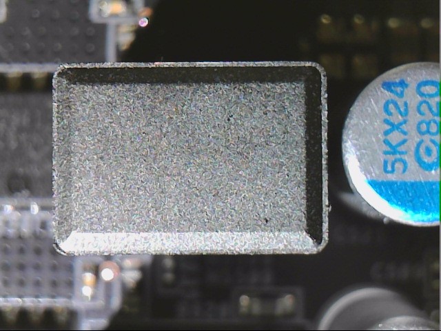
The coils rely on unlabelled ferrite core coils, which have been poured into a case of sintered material. We can already see at this point that this was not a bad choice. With the GPU voltage converters, we suspect the usual 220 nH coils, which make a coil for the memory quite lush at 1 mH.
 |
 |
In direct comparison, the power supply of the memory is quite simple. With the second loop of the PWM controller, the relevant voltage converters are controlled directly, with the high-side relying on an SM4336 and the low-side on an SM4373. This is a simple, single-phase buck controller that is fed from the PEG.
 |
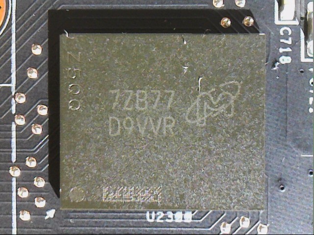 |
The memory comes from Micron and not from most of Samsung’s other RX 580s. The MT51K256M32HF-60 N is a total of eight simple 8Gb modules GDDR5 (256Mb x32) with 6.0 Gb/s at 1.35V nominal operating voltage.
ASRock also relies on a single BIOS, probably also for cost reasons. The position of the chip and its power supply directly below the edge of the GPU socket is rather unusual, because so the BIOS is actually located in one of the suspected hotspots.
We will see later whether this might even become critical, or not.
- 1 - Einführung, Unboxing und technischen Daten
- 2 - Platinenlayout und Spannungsversorgung
- 3 - Gaming-Performance 1920 x 1080 Pixel (Full-HD)
- 4 - Gaming-Performance 2560 x 1440 Pixel (WQHD)
- 5 - Leistungsaufnahme im Detail
- 6 - Temperaturen, Taktraten und Wärmebildanalyse
- 7 - Kühlerdetails und Geräuschentwicklung
- 8 - Zusammenfassung und Fazit


Kommentieren