


Well, meanwhile there are several leaks of “pre-release” models of the upcoming GeForce RTX 3080, but I don’t really trust the roast published here, because I just assume design validation samples. And before I think about how to explain the 350 watts to you, I have created a simple super projection (and cut it a bit on the right side for clarity), which of course has no artistic value whatsoever like several render images, but raises very legitimate questions. I had reported that there are two boards, of which the PG133 is used exclusively for the Founders Edition (FE) and the PG132, which will be the reference for the board partners.
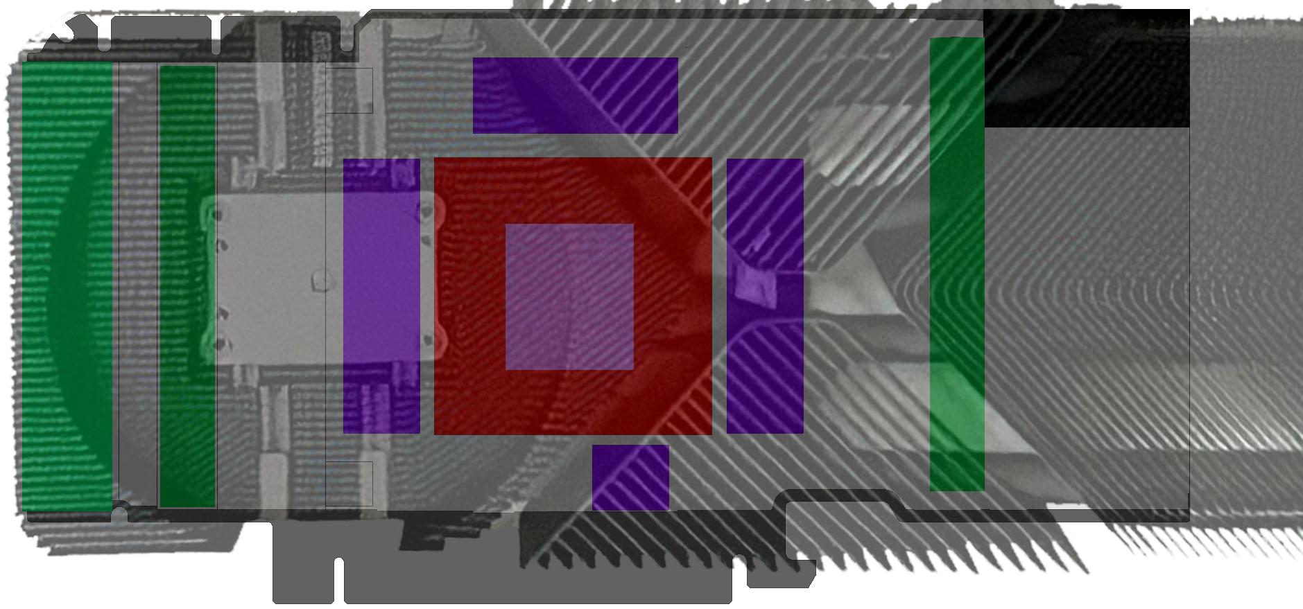
Leaked cooler vs. PG132 and the chip size of the GA102
If one now takes the experiences of the last few years as a guide, places the memory closer to the BGA according to the usual memory manufacturer’s specifications for the tracks and also groups the memory around the BGA for the first time in the only plausible 4-3-4(+1) scheme, then there would hardly be any space left for the display connections on the cooler shown on the Internet, let alone for the necessary voltage converters. The large Turing cards already use a double-sided voltage converter layout, which makes absolute sense considering the hotspots.
If one assumes that for electrical reasons certain minimum distances between the boards and even the individual components must be kept, the distribution based on the leaked cooler would not be possible at all, unless the PG133 of the Founders Edition would completely deviate from the “alternative” reference for the first time. This is of course quite possible and would also give the FE a certain exclusivity, but it would also be an extreme cost driver. All this is very well possible.
My projection, which I have created from memory, should, however, in terms of PG132 (and only this one!) after deducting all possible inaccuracies, be pretty much the same as what Nvidia has already provided to the board partners as a Thermal Design Guide. These things almost always resemble each other, and also the circulated 21.3 cm length falls exactly into this scheme. But I would never publish such originals anyway, as traffic-bringing as that may be. It’s just not appropriate, even if you haven’t signed an NDA for it.
I have placed the chip in the drawing correctly, at least in relation to the board size. TechPowerUp writes on the homepage in the database entry for the GA102 about 700 mm² and is not even very wrong. If you add up all the facts you already know, then with a little bit of calculator and additional information from beloved sources you get a chip area of just over 627 mm², which should be correct.
It is also a fact that there is enough space for the two power supply connections I predicted, because everything that needs to be cooled is first of all supplied in form of electrical energy. Which brings us to the power consumption. And this is exactly where we want to calculate together.
How 230 watts become 350 watts
The professional has two terms at hand when it comes to specifying the total power consumption of a graphics card. Besides TBP as Total Board Power, there is also TGP as Total Graphics Power from Nvidia’s point of view. It deviates a bit in small details (TGP without 3.3 Volt), but at least it still comes up quite well in terms of the orders of magnitude. Do you remember my article “Power Consumption: TDP, TBP and TGP for Nvidia and AMD graphics cards calculated with destruction of a PR foil” ? You should read it again for better understanding.
Some people in forums have been hostile to my estimation (ok, it was rather a nice bird’s twitter) with the 350 watts for the large and the 320 watts power dissipation for the two smaller cards, but I don’t want to comment on the reasons for the lack of understanding. But power comes from fuel and even without “songbirds” the power consumption could be estimated quite well.
So I’ll stick with the 350 to 320 watts and want to calculate down how much could still be allotted to the chip. And this is where it gets interesting, because you can extrapolate voltage transformer losses, low voltages and other things quite well based on the last generations. Well, I asked explicitly for the memory, I am not a clairvoyant.
| Estimated Power Consumption / Losses |
|
| Total Graphics Power TGP | 350 Watts |
| 24 GB GDDR6X Memory (GA_0180_P075_120X140, 2.5 Watts per Module) | -60 Watts |
| MOSFET, Inductor, Caps NVDD (GPU Voltage) | -26 Watts |
| MOSFET, Inductor, Caps FBVDDQ (Framebuffer Voltage) | -6 Watts |
| MOSFET, Inductor, Caps PEXVDD (PCIExpress Voltage) | -2 Watts |
| Other Voltages, Input Section (AUX) | -4 Watts |
| Fans, Other Power | -7 Watts |
| PCB Losses | -15 Watts |
| GPU Power | approx. 230 Watts |
The 230 watts are actually quite mannerly for such a computing monster, if you imply that the clock is also extended here. The fact that the smaller cards are 30 watts less in the TGP is due to the lower memory capacity and the possibly higher clock rates. But we know exactly that from the Titan RTX and the Quadro RTX 6000.
The two smaller cards will probably have one or two memory controllers less, which also suggests different sizes of the CUDA cores. 11 modules are even easier and safer to install than 12 and we still remember the underfill gate of the RTX 2080 Ti. The fact that the TGP is given the same size at the end may be due to the higher clock rate of the smaller models.
As I said, some things are certainly speculative, logically deduced or at least boring arithmetic, but I can also assure you that I don’t like to go out of my way when the balance could be disturbed by unnecessary carelessness or overconfidence. And there are some things I will not write because it is just not done. Or I have to hide things diplomatically. Even if I now fight for readers on the other side of power, no one will try to lure me out of my reserve. 🙂
Also interesting: Exclusive info about NVIDIA’s Ampere: 3 models, memory size, PCBs, an extremely expensive cooler for the FE and the search for the leak


Kommentieren