


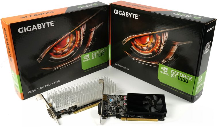
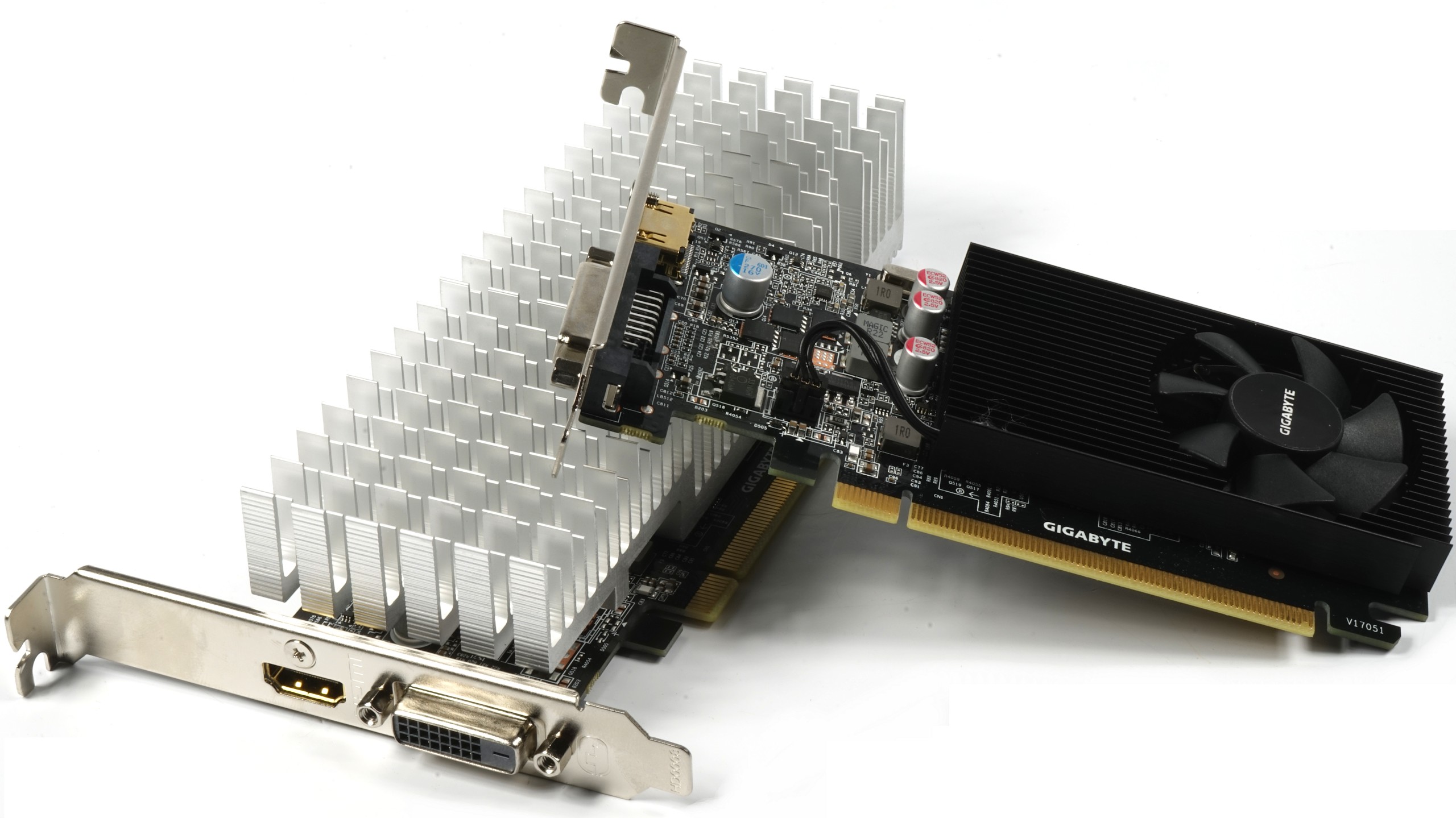
Gigabyte GT 1030 Low Profile and Low Profile Silent
We have deliberately opted for the low-profile form factor, as this type of card is likely to be used mainly in the area of small and very small PCs. And this is exactly where we will start in detail, because with these two gigabyte cards, whose board is completely identical, we can test and compare both the active and the passively cooled version. Is passive operation really possible and sensible this time? We'll find out, of course!
More about GeForce GT 1030
While the GeForce GTX 750 Ti still has five SMX (streaming multiprocessors), the GT 1030 is equipped with only three such SMX. With 128 CUDA cores per SM/SMM in the Pascal and Maxwell architectures, that's 384 cores for the GT 1030 and 640 cores for the GTX 750 Ti. Both designs have eight texture units per SM, a total of 24 on GeForce of the GT 1030, while the GTX 750 Ti still has the 40.
The two GPUs have a pair of ROP partitions and process up to 16 32-bit integer pixels per bar. However, these partitions are connected to the 256KB L2 cache on the GP108 and 1MB L2 cache on the on GM107. In the end, this means that the GeForce GT 1030 can only have 512KB L2 cache, which means a huge step backwards to the GTX 750 Ti. And while the GeForce GTX 750 Ti has two 64-bit memory controllers, the GT 1030 has only one pair of 32-bit controllers for the memory bus, resulting in a 64-bit interface. Here, the GT 1030 loses a lot of resources, which is in no way proportional to the only approx. 4% reduced complexity of the chip as such.
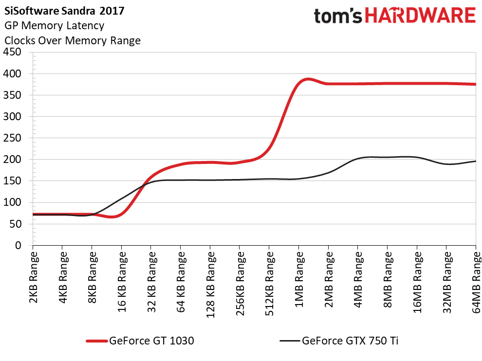
Nvidia, of course, tries as usual to compensate for these deficits of the GT 1030 with higher clock rates. Our test pattern uses a base clock of 1227 MHz and boosts at least 1468 MHz. In contrast, the GeForce GTX 750 Ti starts at 1020 MHz base clock and only increases to approx. 1085 MHz. Of course, a narrow 64-bit memory bus clips the peak bandwidth of the GT 1030 to 48 GB/s at 6Gb/s GDDR5. In contrast, the wider interface of the GTX 750 Ti allows up to 86.4 GB/s. The consequences can be seen all too clearly in the diagram. But what can we compare the GT 1030 with, if not the GTX 750 Ti?
The GT 730 as a brother in spirit?
Let's remember: the GTX 750 (Ti) was started at the time as a 130- to 150-euro card and you get leftovers still offered for up to 100 euros. We had chosen them at the beginning, because the number of transitors of the used GM107 roughly corresponds to the number of GP108 on the GT 1030. In reality, however, the GeForce GT 1030 and gt-730 are the real brothers in spirit, because Nvidia has never released a 900 product below the GeForce GTX 950. In the end, the Kepler-based GeForce GT 730 has a much tighter match with its 384 CUDA cores and 16 texture units (over two SMX), the eight ROPs, the 512KB L2 cache, and a 64-bit interface.
The power consumption of the GT 730 with 38W is also not far from what Nvidia now indicates with the GT 1030 with 30W. After all, the GeForce GTX 750 Ti is a 60W to 75 watt card that never really came on the market as a passive card. But why is the GP108 so much more complex than the GK208? The architectures are simply no longer the same, so much as a starting point.
The GT 1030's GP108 uses a single Graphics Processing Cluster with three SMX. Each of the SMX has 128 CUDA cores, eight texture units, 24KB L1/texture cache, and 64KB common address space. The GK208 of the GT 730 has two SM with 192 CUDA cores each, eight functional texture units, 64KB shared memory and L1 cache, and a separate texture cache. The GP108 has over 16 ROP units, the GK208 over eight.
In the end, the GP108 offers a much higher pixel filling rate than the GK208 (19.8 GP/s vs. 7.2 GP/s), but the texture rate has also grown significantly (29.8 GT/s vs. 14.4 GT/s). Nvidia has also justified the higher number of transistors by the fact that significantly more resources are needed for the much more aggressive clock rates, as well as the correct asynchronous calculation support via the dynamic load distribution. The GeForce GT 1030 uses a complete, uncut GP108 processor – so there are no disabled resources to turn on. Only the density and complexity is thus significantly higher.
AmD's competition with the Radeon RX 550 technically lands somewhere between GM107 and GK208. The Radeon RX 550 is a little more expensive and requires slightly more electrical power than the GeForce GT 1030. We also have low-profile and "single-slot" versions on the Radeon RX 550, but not both in one. And also no serious card with passive cooling. On the other hand, the Radeon RX 550 even contains 512 stream processors, 32 texture units and 16 ROPs in the Polaris 12 chip, which combines 2.2 billion transistors.
This means that the Radeon RX 550 achieves a pixel filling rate of 17.6 GP/s and a texture rate of 35.2 GT/s. Faster 7Gbps GDDR5 modules on a much wider 128-bit memory bus also give the AMD card a theoretical bandwidth advantage of a whopping 233%! Like Mvidia on the GK108, AMD has also reduced PCIe 3.0 support. Instead of the 16 lanes, there are now only four lanes left.
But Nvidia is sure to beat the AMD card with the GT 1030. at least achieve a tie. Our tests have to prove whether this very self-confident announcement comes up. In addition, Gigabyte is sure that he has hit the nerve of the times with the passive solution. Of course, we will come to the benchmarks and measurements that can clarify these statements in detail.
| Gigabyte GeForce GT 1030 Low Profile (Silent) |
AMD Radeon RX 550 (Reference information) |
|
|---|---|---|
| Chip: | GP108 | Polaris 12 |
| Transistors: | Eel 2.2 billion | Eel 2.2 billion |
| Shader Units: | 384 | 512 |
| GPU base clock: | 1,228 MHz | 1,100 MHz |
| GPZ Boost clock: | 1.468 MHz | 1,183 MHz |
| TMUs/ROPs: | 24/16 | 32/16 |
| Pixel fill rate: | 26.7 GPix/s | 18.9 GPix/s |
| Texel filling rate: | 40.1 GTex/s | 37.9 GTex/s |
| Amount: | 2,048 MB GDDR5 | 4,096 MB GDDR5 |
| Memory clock: | 3,000 MHz | 3,500 MHz |
| Memory interface: | 64 Bit | 128 bits |
| Memory bandwidth: | 48 GB/s | 112 GB/s |
| Power consumption: |
30 watts | 50 watts |
Test system umd measurements
The new test system and the methodology we have already described in great detail in the basic article "So we are testing graphics cards, as of February 2017" and so, for the sake of simplicity, we now only refer to this detailed description, which is modified form can also apply to the CPUs. So if you want to read everything again, you are welcome to do so.
In this case, only the hardware configuration with CPU, RAM, motherboard, as well as the new cooling is different, so that the summary in table form quickly gives a brief overview of the system used here and today:
| Test systems and measuring rooms | |
|---|---|
| Hardware: |
Intel Core i3-6320 MSI Z270 Gaming Pro Carbon G.Skill F4-3200C14Q-32GTZ en 2133 MT/s (16GB installed) 1x 1TB Toshiba OCZ RD400 (M.2, System) 2x 960GB Toshiba OCZ TR150 (Storage, Images) Be Quiet Dark Power Pro 11, 850-watt power supply Windows 10 Pro (Creators Update) |
| Cooling: |
Noctua NH-D15 Thermal Grizzly Kryonaut (for cooler change) |
| Monitor: | Eizo EV3237-BK |
| Power consumption: |
non-contact DC measurement on the PCIe slot (Riser-Card) non-contact DC measurement on the external PCIe power supply Direct voltage measurement on the respective feeders and on the power supply 2x Rohde & Schwarz HMO 3054, 500 MHz multi-channel oscillograph with memory function 2x Rohde & Schwarz HZO50, current pliers adapter (1 mA to 30 A, 100 KHz, DC) 2x Rohde & Schwarz HZ355, probe divider (10:1, 500 MHz) 1x Rohde & Schwarz HMC 8012, digital multimeter with storage function |
| Thermography: |
Optris PI640, infrared camera PI Connect evaluation software with profiles |


Kommentieren