


What is it about and what is a package?
Since the GPU (and in this case also the interposer with GPU and memory) cannot be soldered so easily onto the PCB, these components are first used by one of the specialized finishers (e.g. ASE in Taiwan) is transported to a so-called package in the flip-chip process ("packaging process"), which can later be processed much more easily in the factories.
To do this, it is important to know that these packages are fed by machine from a roll on a kind of transfer tape in the SMT process and then positioned on the PCB. But this is precisely where serious problems existed in advance, because many, especially older SMT systems, were unable to transport and position these highly sensitive components without damage. As far as the theory…
 The mother of the Vega packages: uncast and made in Taiwan
But let's first compare the package as it was initially used on AMD's internal slides and demonstrations (pictured above) and as we find it in a similar form on our RX Vega56. We can see that there are deeper gaps between the GPU and the two memory modules, as in Fiji, respectively. these components are relatively high.
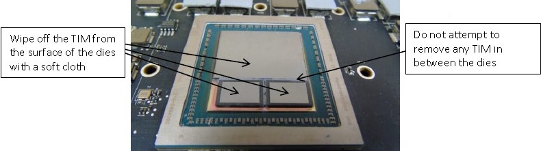
The interposer, on the other hand, is extremely thin and, above all, fragile. Hence the warning in AMD's slides for the developers and industry, as well as all internal stakeholders, e.g. when removing old thermal paste during the development phase, to work very carefully.
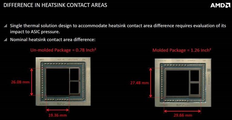
Differences between the individual packages
For a machine production, such a thing is of course also quite risky, especially since one can also encounter so-called "underfill" problems, since in packaging also pressure-sensitive cavities can always form between the interposer and the intermediate board. This can be counteracted by additionally relying on the so-called molding, i.e. the additional shedding of the chips and memory modules on the interposer. Now let's look at the schema for each of the two variants:
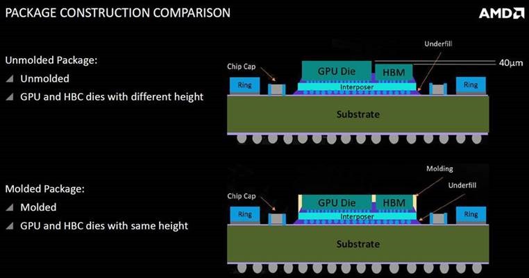
However, if you look at the package currently used on the Vega FE and some RX Vega (picture below), you can clearly see that AMD is now relying on molding here. The area around GPU and memory has been poured over a large area with a suitable material, which significantly increases stability. This package is again Made in Taiwan and is manufactured by ASE.
 Variant Two: shed and again made in Taiwan
A third variant comes into play
Nevertheless, AMD is currently demonstrably using both variants of the package (which now come from two different finishers), which could well pose technical problems for some AIb, which we want to address in a moment. But what is different about the third variant, which we e.g. also found our RX Vega56? Apart from slight optical differences in the ring, the board and the label, the manufacturing location and finisher are also different.
 Variant three comes from Korea and obviously does not come from ASE
Let's remember a little bit. In the past, for example, It was usually the case at Fiji that AMD only sent the working chips to the storage supplier SK Hynix and they installed functional HBM modules there, but had the packaging done immediately in Korea without molding and only then the package was sent back to AMD. The gemed packages on our two previously tested maps come from ASE in Taiwan, but here a Korean packaging comes into play again.
But where is the problem?
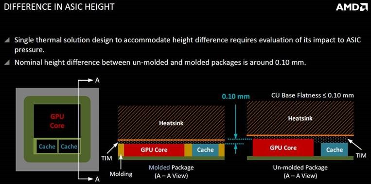
Since the HBM2 is 40 microns lower in the unfinished packages and the underfill of the third variant obviously differs somewhat, the AIB face new challenges. On the one hand, in mass production and when using a common cooler for several models, care must be taken to ensure that the thickness of the applied thermal conductive material must be optimised in the case of unmodified packages, that the viscosity must be high enough, and that the nevertheless, the contact pressure resulting from screwing does not damage anything.
In our own experiment, we compared both PCBs against each other, each of which runs cards with a predefined power limit in such a way that they run in the same gaming loop approx. 260 watts of power. The slightly more viscous Diamond from Innovation Cooling was used as a paste compared to the rather thin cryonaut from Thermal Grizzly.
In order to get a similar heating curve for both packages under load, the Diamond actually had to use a slightly higher contact pressure for the lower package (between approx. 0.05 and 0.1 Nm more). Since many manufacturers also work with stoppers to prevent overturning, this can become a problem if suddenly the torque is no longer sufficient, because e.g. the threads are finished.
In the case of the significantly more liquid cryonaut, however, it did not matter which of the two packages was used at identical contact pressure. Unfortunately, it is the case that not so viscous pastes are rather not suitable for industrial use with pre-assembled application on the heat sink.
We also have information that individual partners now have to attach the radiator heatsinks with six instead of four screws and accordingly also all previously prefabricated heat sinks and backplates for the uncast packages. had to be adjusted, or were no longer usable. Others reported SMT problems and other adjustments, which could delay the appearance of some custom models.
AMD, in response to questions from board partners, stated that the minimal differences between the packages should not affect the functionality of the individual cooling solutions already developed. But even if this proves to be a fact, the finishers must first run their own test series in their own interest in order to prepare mass production as optimally as possible. And this again costs time, which no one actually has. While the first Custom models were already announced for mid-September, some models are now likely to be delayed until the end of September or the beginning of October.
Is it due to the different memory?
We will try to find out more details, as the current rumors range from the use of various memory modules from Samsung and SK Hynix, depending on the package type. However, as long as there are no reliable statements made by directly interested parties in this regard, this will of course remain purely speculative for the time being. But it would also be one of the possible reasons why we can see different heights of HBM2 memory modules in the packages and why there are different productions.
It is also technically not easy or it is almost impossible to pour in such different-sized components cleanly, which also speaks to the presumption that different memory modules could be used here. A pure capacity problem in the packaging process should actually be ruled out at the moment.
 On one of the unnamed packages there was a label on the HBM2
Update, Aug 22, 2017, 10:30 a.m.
As we have just learned from a fairly secure source, the RX Vega56 only uses the HBM2 from SK Hynix. Nevertheless, two package types are also to be in circulation for the RX Vega56, which cannot be ordered separated by the AIB, so that one cannot orientate oneself towards a package type. However, the 0.1 mm difference in height is by no means a negligible size.
How relevant is the whole thing?
Here, the spirits of the finishers differ somewhat, because those who are equipped with newer, suitable production systems have fewer problems with the production of boards. In the case of the coolers, on the other hand, it depends on the individual solution, the potential modification of which could also mean higher costs, since much of what was planned has to be re-dissolved and manufactured.
An important factor is also time, because every day lost costs cash. If different HBM2 memory comes into play, it will be interesting to compare the possible overclockability and heat generation of the modules. We are definitely sticking to it.


Kommentieren