


AMD has carried out the long-awaited presentation of Navi as part of the E3 and has already explained the most important thing during the event. Nevertheless, some questions remain unanswered, which I will have to clarify in the coming days or weeks. Unfortunately, this also includes AMD’s (new) information policy, not having written appropriateletters to all media in advance. AMD cites an RRP of 449 USD for the Radeon RX 5700XT, or 379 USD for the Radeon 5700. The market launch is announced for 07.07.2019 and thus at the same time as the new Ryzen CPUs.
Details about the new Radeon RX 5700 and RX 5700 XT
The Radeon RX 5700 XT has 2,560 stream processors and 160 texture units divided into 40 computing units. With a maximum boost clock of 1,905 MHz, these CUs enable up to 9.75 TFLOPS of computing power. On paper, the card would then lie somewhere between a Radeon RX 590 and a Radeon RX Vega 56. However, AMD sets slightly different clock rates this time, so the boost frequency can only be a kind of vanity rating.
The more realistic specification is 1.755 MHz. AMD says that this game clock rate represents a typical one in over 20 games that you have tested yourself and therefore you expect the cards to run somewhere between this game and the boost frequency. A 1,605 MHz high base clock, on the other hand, should always be guaranteed, even in a worst-case workload such as Furmark.
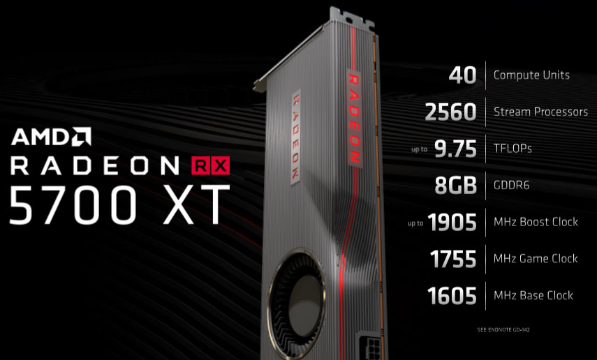
AMD combines the Radeon RX 5700 XT with 8GB of GDDR6 storage, transmitting 14Gbps data over a 256-bit bus. The resulting theoretical bandwidth of 448 GBps exceeds the 410 GBps available to the Radeon RX Vega 56 via its 8 GB HBM2, but is behind the 483 GBps of the Radeon RX Vega 64.
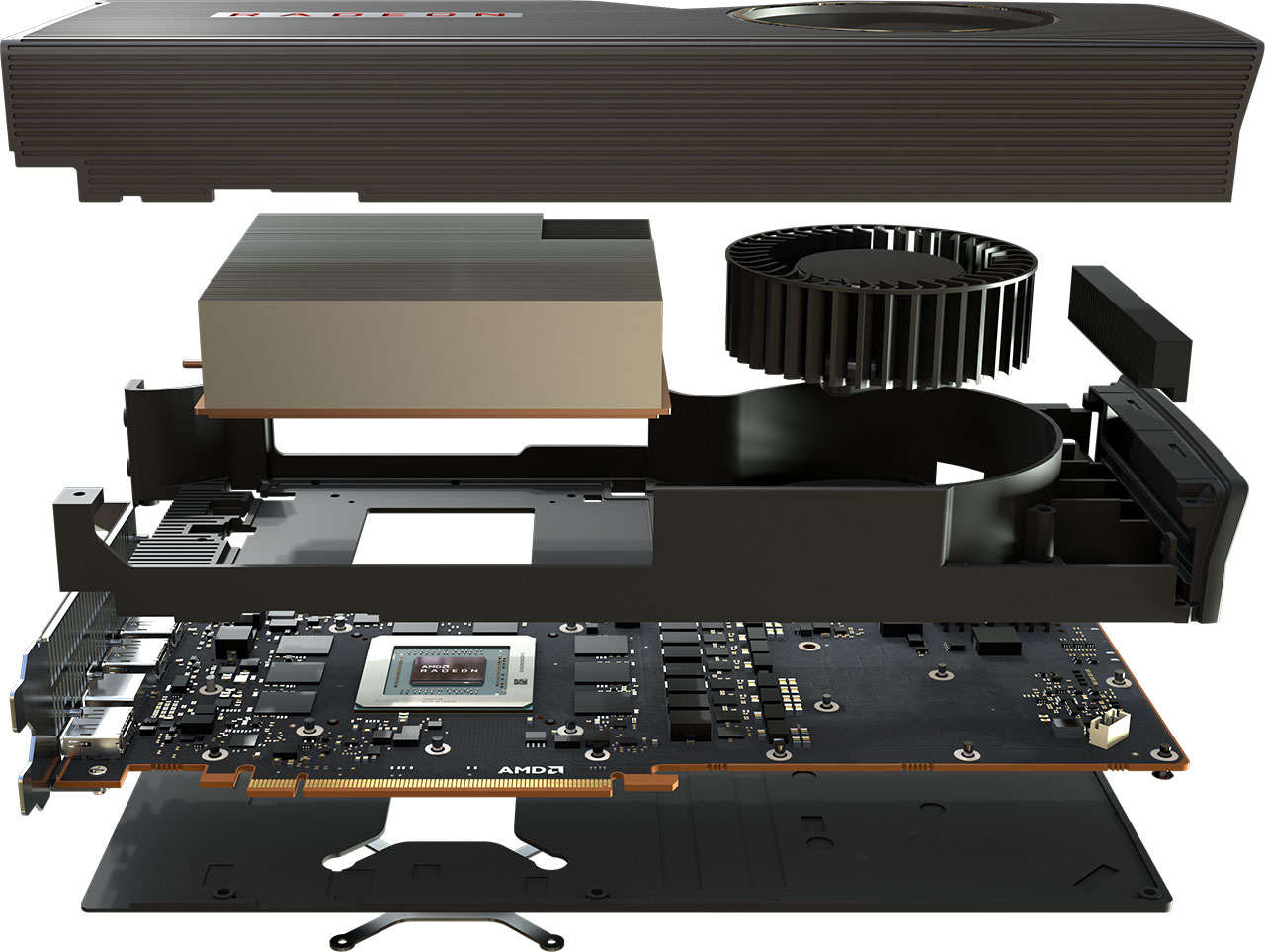
Like its previous reference designs, the AMD-owned Radeon RX 5700 XT will be a dual-slot implementation with a radial fan that blows air through an aluminum lamella heatsink that sits on a vapor chamber as usual and where the waste heat is applied to the slot panel can escape the card (Direct Heat Exhaust). Many enthusiasts are quite critical of this solution, as it is usually louder. However, we estimate exactly this property compared to axial fans, which dissipate the heat energy back into the interior of the PC housing.
AMD also assures us that the fan speed would be carefully controlled to keep the sound level below 43dB(A). A housing and a back plate made of aluminum alloy cover the front and back of the card, while the high-quality graphite phase change pad ensures maximum heat transfer from the navigation chip as usual.
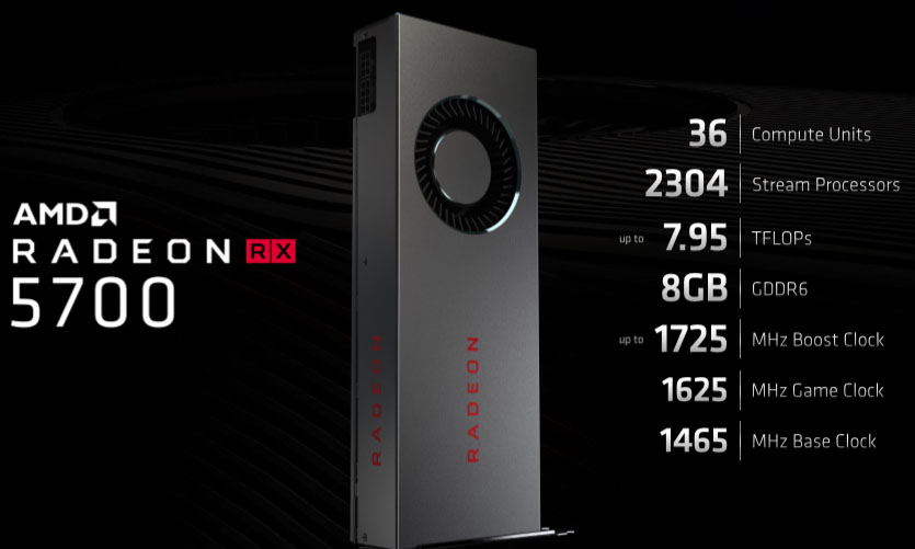
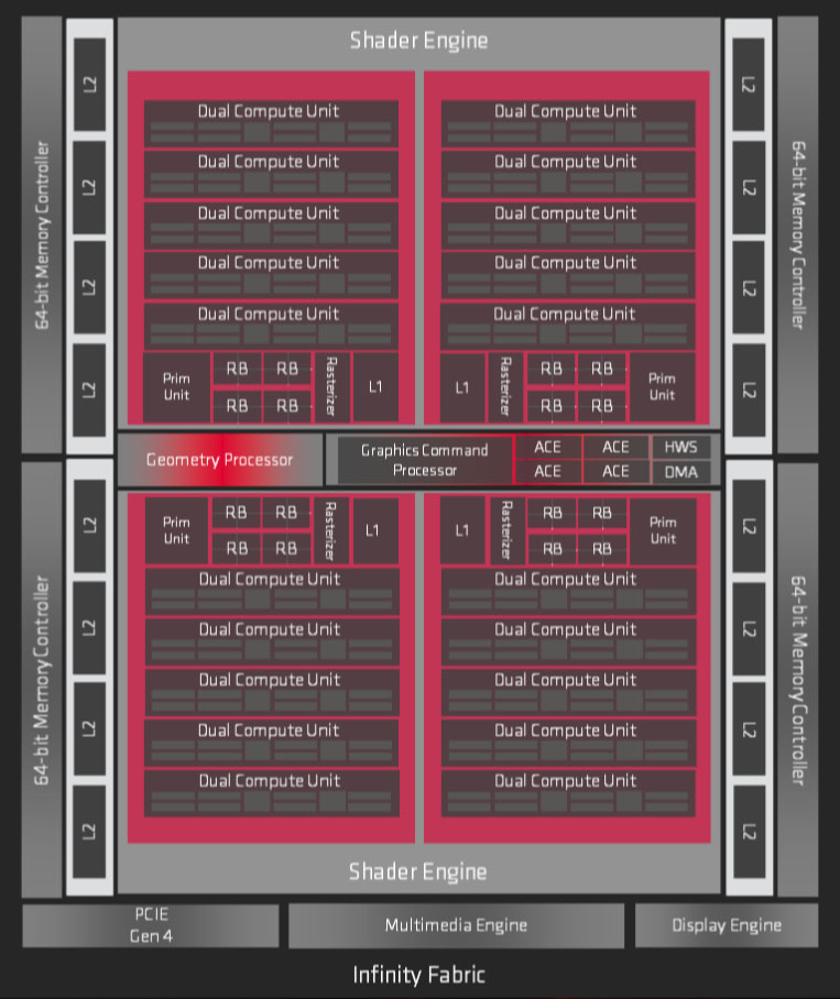
The reference card of the Radeon RX 5700 receives a relatively small incision and loses four CUs and thus 256 stream processors compared to the XT variant. The remaining 2,304 ALUs and 144 texture units operate at a typical game clock rate of 1,625 MHz and 1,465 MHz base clock. AMD says that the RX 5700 can reach a boost clock of 1.725 MHz and that’s exactly why you calculate the up to 7.95 TFLOPS computing power of this card. All 64 NAVI ROPs are retained when the Radeon RX 5700 XT is slimmed down to the RX 5700, as well as the chip’s 256-bit memory bus and 4MB last-level cache.
Both cards support PCI Express 4.0 and thus theoretical transfer rates of 16 GTps. Of course, there are no compatible platforms at the moment, not yet. PCIe 4.0 support for older AMD chipsets was officially lifted earlier this month because of concerns about signal integrity on the motherboards, which were not explicitly designed to enable the standard. But until the Radeon RX 5700 series cards are available, X570-based boards and third-generation Ryzen CPUs should also be ready to provide the basis for the PCIe 4.0-enabled add-in cards.
The two new Radeons are equipped with an eight-pole and a six-pin external supply socket. In the case of the Radeon RX 5700 XT, the specified board power of 225 watts requires this configuration. But the Radeon RX 5700 could probably have come with 2 6-pole or an eight-pin jack for its typical 180W board power. According to AMD, the 5700 XT uses a seven-phase power supply, while the 5700 loses a GPU phase and a total of six phases remain for the GPU and GDDR6 memory.
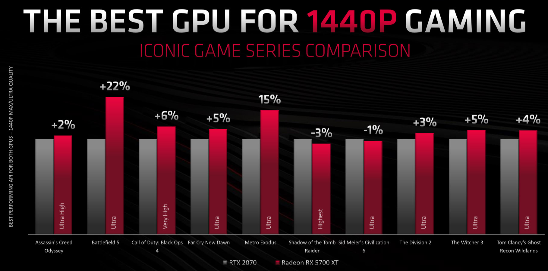
And where does gaming performance come from? As for this performance, AMD announced that the Radeon RX 5700 XT will beat a (reference) GeForce RTX 2070, which also means that it should have no problem displacing the Radeon RX Vega 64 in our benchmark suite. The Radeon RX 5700 is also expected to beat the current GeForce RTX 2060. It’s exactly what I suspected in the video for Nvidia “Super” cards.
Old or new? A quick look at AMD’s new GPU
Navi surpasses the GCN predecessors due to several enhancements built into an architecture called AMD RDNA (Radeon DNA). Although the company says RDNA is completely new, the remains of Graphics Core Next are clearly recognizable. But instead of discussing how much of a graphics processor needs to be changed to talk about a truly new architecture, we should look at something that RDNA really encompasses.
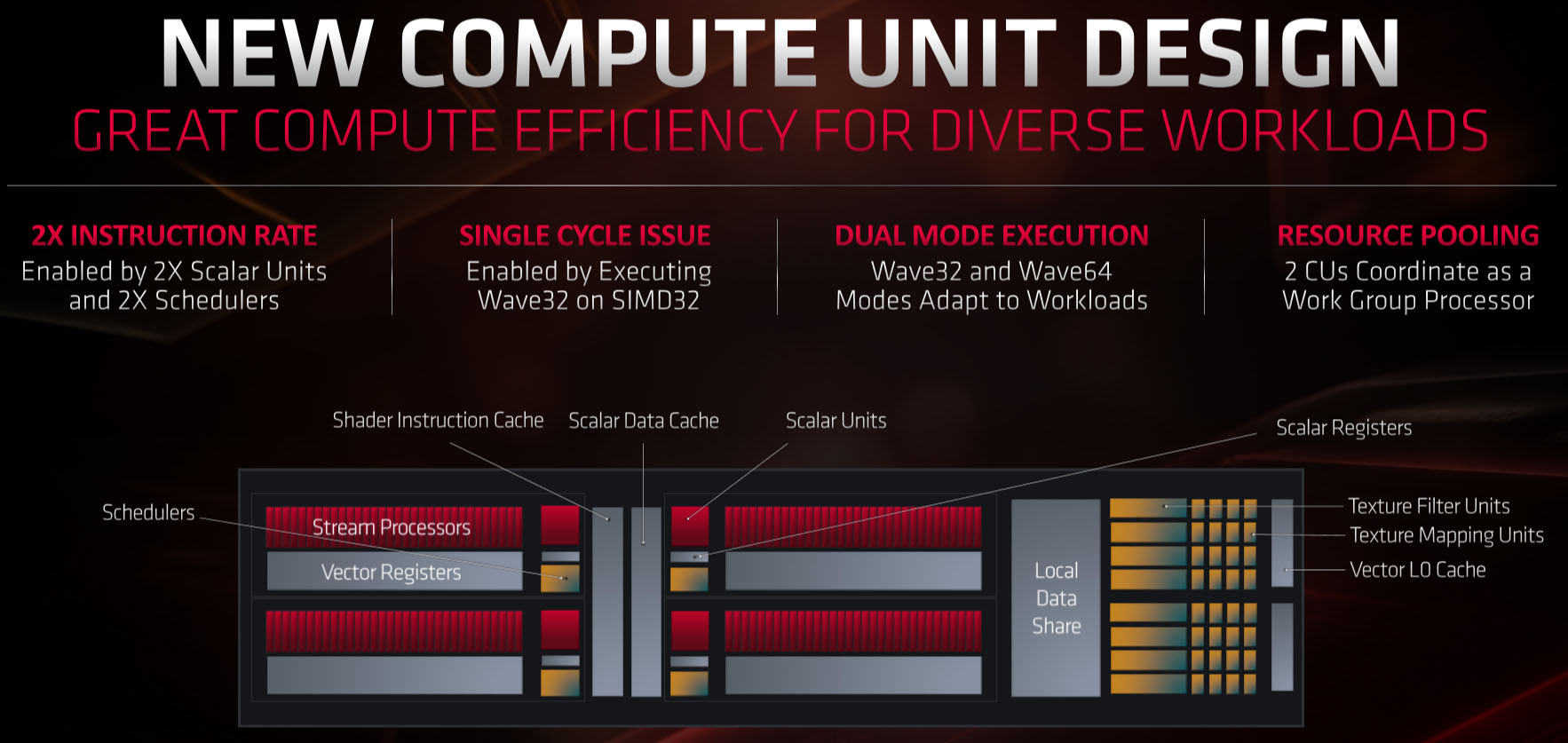
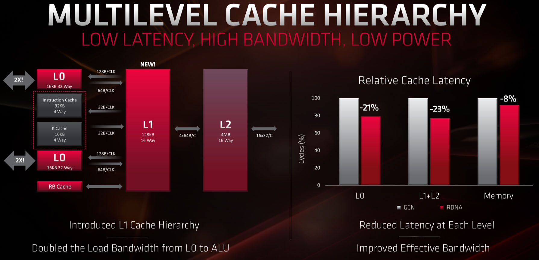
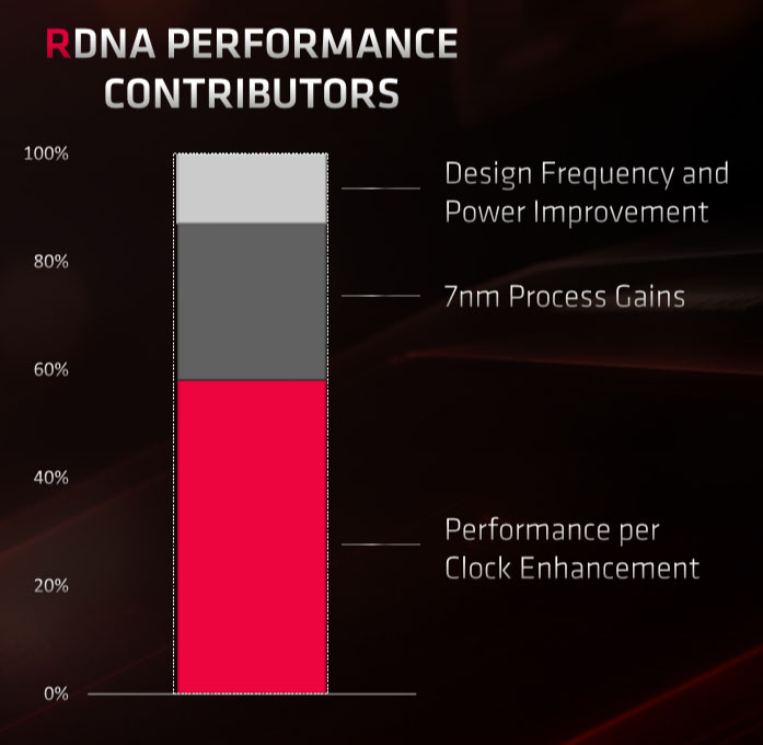
The biggest advantage of this design is the architectural reorganization, which leads to more performance per beat. Significant efforts have been made to make the compute units easier to use for a wider range of workloads. And optimizations for single-threaded performance should turn into lower latency for parallelized tasks. The cache hierarchy has also been enhanced by a new L1 (total of 512KB) and a better delta color compression algorithm that provides more effective bandwidth than the previous generation of AMD.
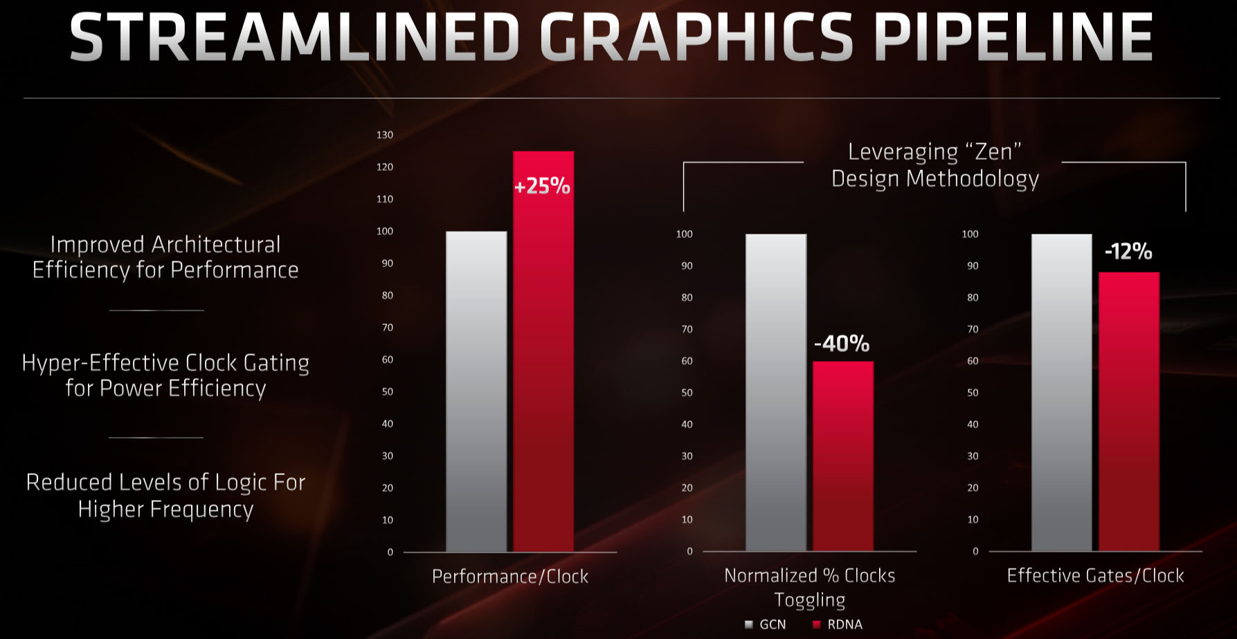
Discussions leading up to the Navi announcement made it clear that AMD was using some of its Zen design methods to improve the graphics pipeline. Clock Gating makes it possible to optimize the performance per watt and thus fix one of Vega’s ugliest defects. As a result, a lower logic per stage also allows significantly higher operating frequencies. Taken together, AMD says these efforts account for about 10% of profits compared to GCN.
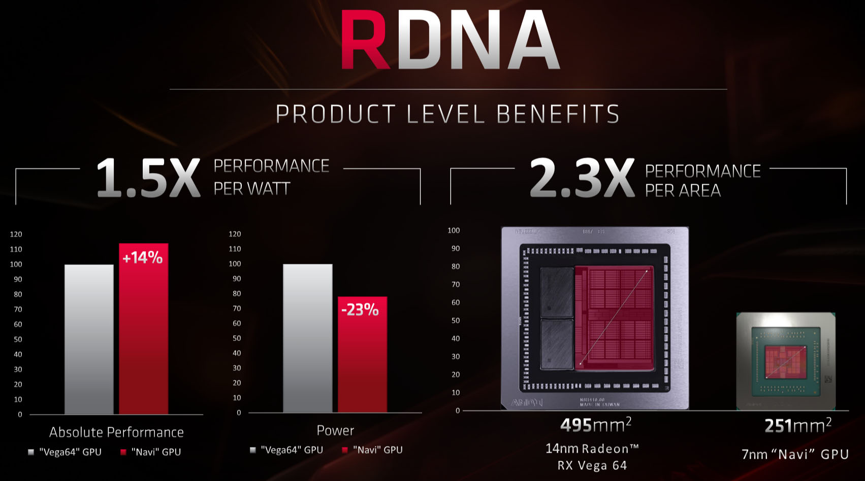
Of course, Navi also benefits greatly from TSMC’s 7nm node and the advantages of the new process technology. The chip consists of 10.3 billion transistors distributed on a 251 mm2 chip. Vega is much bigger. Manufactured according to the 14nm LPP process of GlobalFoundries, it comprises 12.5 billion transistors in a 495mm2 chip.
No wonder AMD has a better frame rate than the Vega 64 with significantly lower board performance.
In addition to the purely 3D-oriented features, Navi also has an improved video engine. Now the fixed-function hardware accelerates VP9 decoding at up to 4K90 and 8K24, the H.264 decoding at 1080p600 and 4K150, the encoding at 1080p360 and 4K90, the H.265 decoding at 1080p360, 4K90 and 8K24 as well as and the encoding at 1080p360 and 4K60. According to reports, the accelerations of the encoder are up to 40%.
The Radeon Display Engine now also supports Display Stream Compression 1.2a, which is important for its ability to operate 4K monitors with refresh rates of over 120 Hz without Chroma sub-sampling. Previously, 3840 x 2160 pixels and 144 Hz required a reduction in image quality to stay below the DisplayPort bandwidth limit. Alternatively, you could also reduce to 120 Hz at 8bpc color depth. And if you use an HDR-enabled monitor, you would have to go back even further to 98 Hz for 10bpc. However, with the advantage of almost lossless compression, AMD can now control 4K monitors with up to 240 Hz or 8K monitors with up to 60 Hz via a single cable without worrying about these compromises.
However, it should also be remembered that monitors must also support DSC in order for the function to work at all. AMD enthusiastically presented a future 43″ DisplayHDR-1000-certified display from Asus with a native UHD resolution and 144 Hz refresh rate, but could not give us any further information, except to mention that there are DSC for single-cable connections will definitely support it.
Currently no Ray Tracing today and somewhat vague outlook for the future
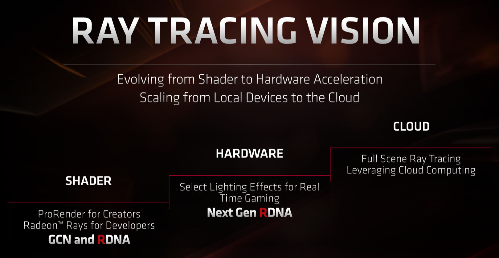
Navi does not include any hardware support for ray tracing in any form. Instead, David Wang, SVP of AMD Radeon Technologies Group, said existing GCN and RDNA-based GPUs would support raytracing via shaders in ProRender (for developers) and Radeon Rays (for developers). Then, along the way, a next-gen implementation of RDNA will (need) to evolve to also accelerate “selected lighting effects for real-time games”.
AMD’s vision is to track radiation through the cloud. Could the company mean that complex calculations are then not realized locally, but as pure stream content for gamers? I cannot imagine that customers will be overwhelmingly enthusiastic about such a proposal. Regardless, AMD expects it will be a few years before this 8,8-time raytracing feature is launched at all.
There is much more to say about the basic architecture of Navi, so today’s article can only be a small and superficial summary and preview. In addition, AMD unfortunately “forgotten” to offer briefings and slides to all relevant editorial offices, so that I also had to resort to third-party material.


Kommentieren