


We've been releasing mountains of salami slices since December and AMD's Tech Summit 2016 in Sonoma, California – and today, vega is the last one, because for AMD, it's really all about the sausage. The tight timetable for 2017 looks the same: packed and hectic.
 In the first quarter we expect Ryzen for the desktop (we already wrote about it), Freesync 2 (we also reported) and throughout the year various server and notebook solutions.
Machine learning will also be a hot topic for AMD – and then, of course, Vega, the hotly anticipated third generation of AMD's GCN architecture.
We will probably be able to expect finished products with these chips at some point in the first half of the year, but no later than the end of June. After the fair is before the fair – and before the Computex it should have happened after all.
Until then, unfortunately, we have to squeeze out again what AMD has given us in advance in terms of information, even if it is not excessive lyant and does not yet include any practical tests. Be that as it may: AMD has revealed a little (theory) and we were also promised more bites just before the real launch of Vega.
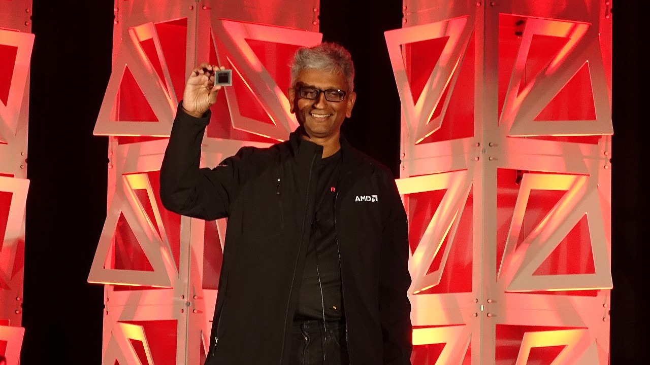
Raja Koduri, senior vice president and chief architect of the Radeon Technologies Group, stood on stage like an excited kid at AMD's Tech Summit and proudly showed us how Bolle was a first chip pattern from Vega, in which in turn over 200 changes and improvements in the redesign of the architecture.
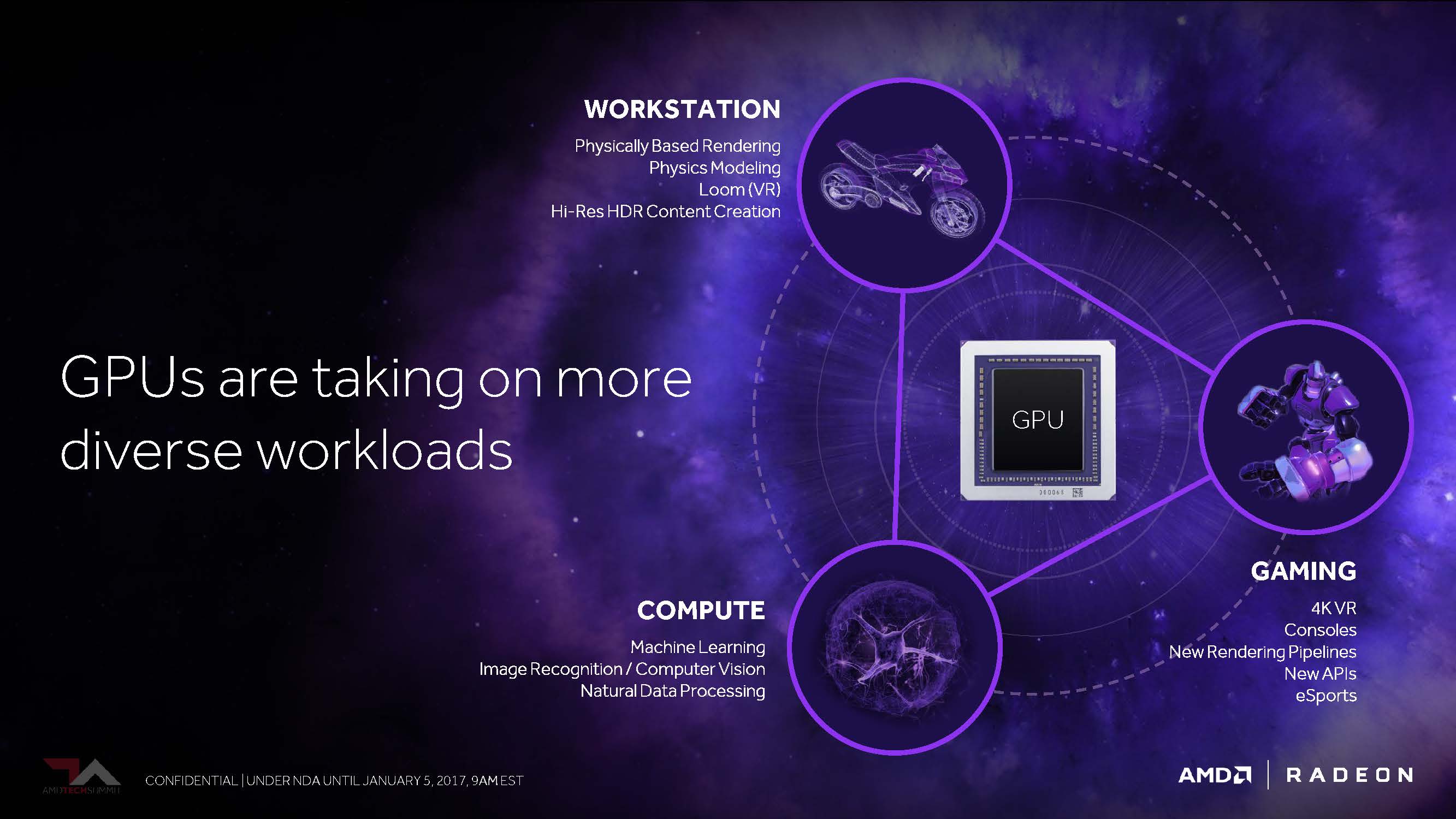
Even if it probably boils down to a new generation of GCNs, AMD has never tired of stressing that it will be a completely new solution. You could even believe that, because it doesn't just take into account the benefits that directX 12 is expected to bring, but also what Nvidia used to play under DirectX 11, and where you've seen and seen some catching up to do when it takes on the consistent exploiting the resources.

To give us a first taste, however, Koduri limited himself to what he considered to be the most important and limited the selection of appetizers to a whole four designs, which, however, could well have it in themselves as technical calorie brooms. Of course, we are happy to pass on this rather manageable plate of the four delicacies to our readers.
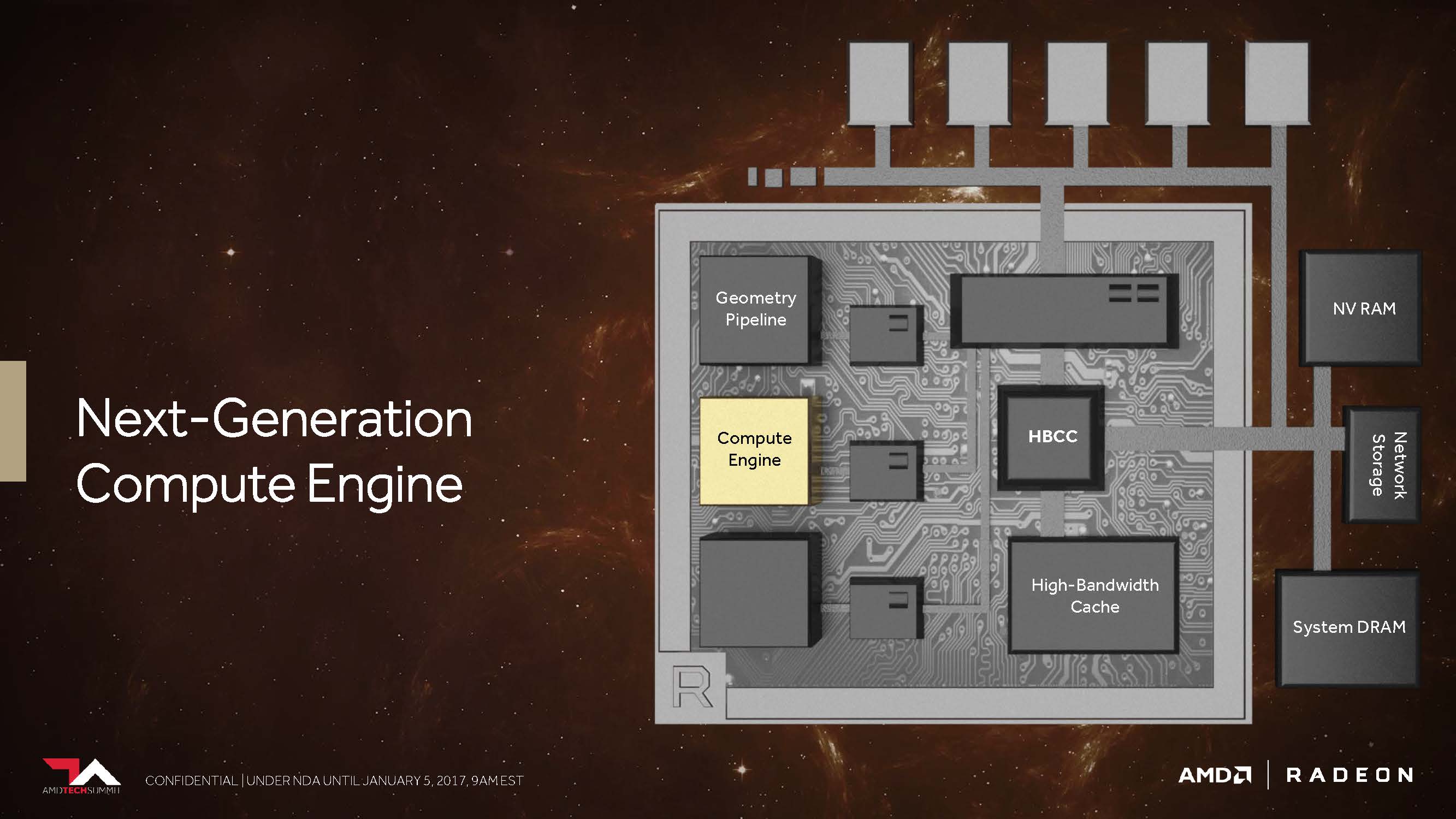
1. HBM2 as a scalable storage architecture
As the first clue to Vegas's architectural change, Koduri referred to the available storage and the entire associated infrastructure.
He made a strong start by showing us how the memory requirements of the games have developed on the desktop PC in recent years and how the workloads in professional applications have developed right down to the petabyte range and in machine learning and training. have even moved to the exabyte range, or will be moved. To do this, he also mapped the relationship between performance increase and corresponding memory requirements.
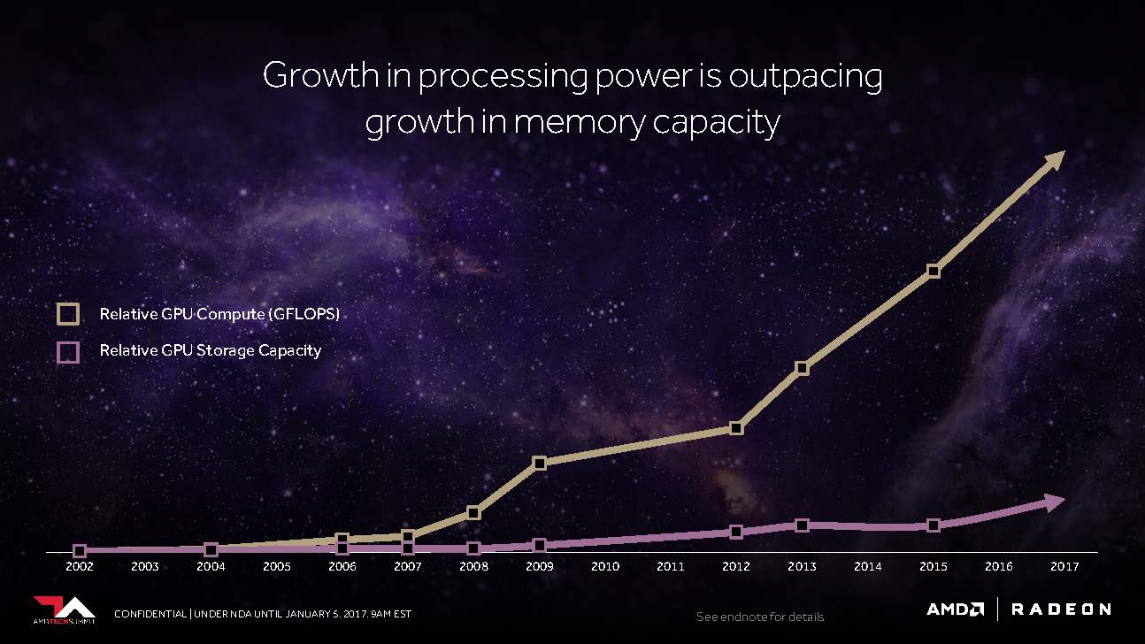
AMD and Nvidia are both working (each on their own) to reduce host processor overhead and maximize throughput, minimizing bottlenecks in accessing the GPU, especially those that, given the extensive data sets occur again and again (can).
It is therefore important to bring even more memory capacities even closer to the GPU and not to let the costs explode. It seems that AMD Vega has moved a big step closer to this important goal with a much more flexible storage hierarchy.
The fact that Vega can and will use HBM2 is no longer a secret. But AMD has at least explicitly confirmed here what you can already see on the whole roadmaps of the past year. could have suspected. But one becomes more concrete and calls this accumulation of on-package memory, which was formerly quite unspectacularly called a frame buffer, now brilliantly "High Bandwidth Cache". Nice catchphrase – but what does AMD actually imagine?
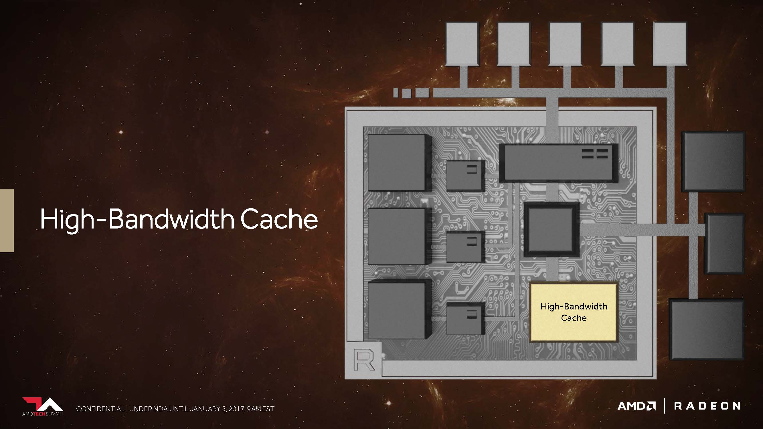
If you follow the words of Joe Macri, Corporate Fellow and Product CTO, HBM had the vision to bring the most powerful memory as close as possible to the GPU. This, he says, also includes the working and data storage of the entire system – giving the above-mentioned new "High Bandwidth Cache" a little more fodder.
And even if this includes much slower technologies in this infrastructure, we want to see HBM2 further than what it really is: a significant step forward.
An up to eight-fold increase in the capacity of each stack in direct comparison to the first generation should also be able to finally put a break on the future of the Radeon R9 Fury X – especially since the doubling of the bandwidth per pin helps significantly increase the maximum possible throughput of the whole.
You can also see it this way: If AMD were to use the same 4-Hi stacks with HBM2 memory clocked to 700 MHz as Nvidia did on the Tesla P100 accelerators, then Vega would have a 16-GByte card with a whopping 720 Gbps, with enough air for both even higher storage capacity and bandwidth.
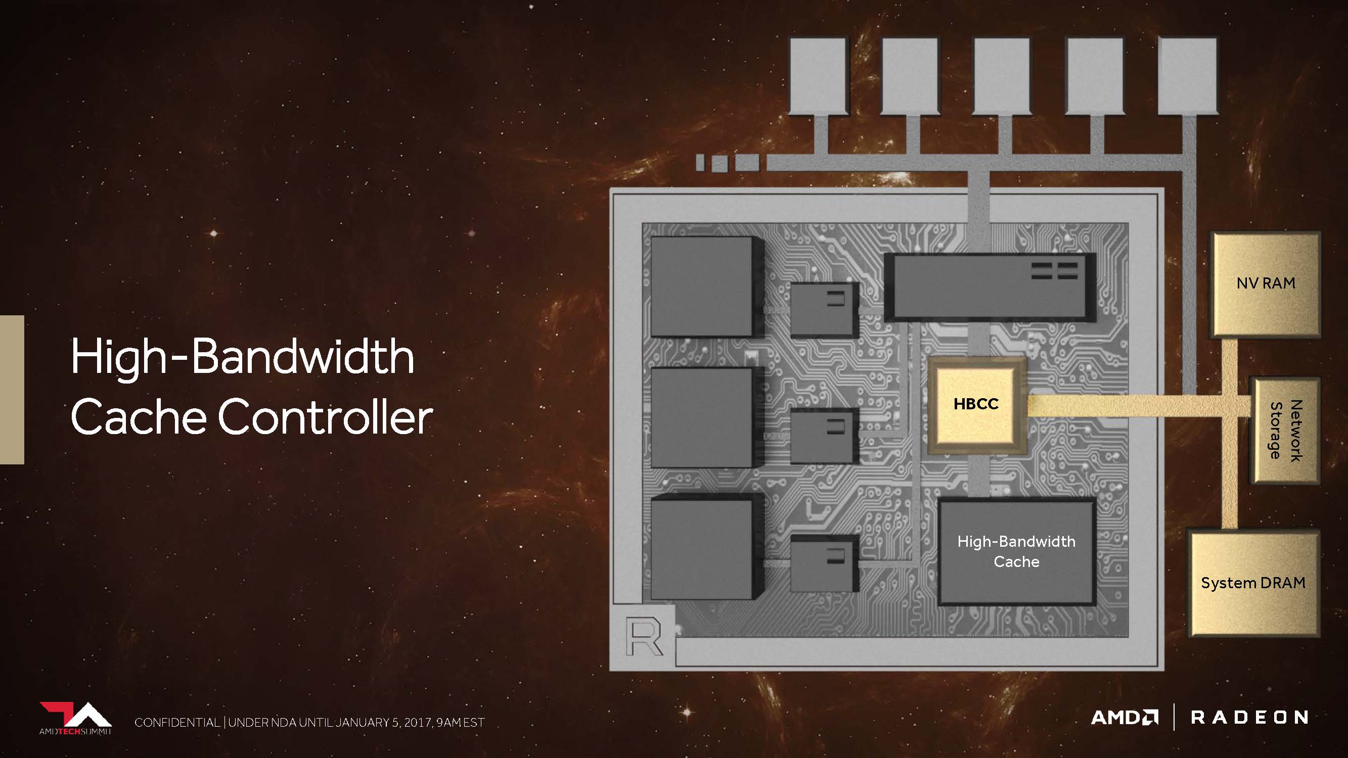
We think this should have the greatest impact on gaming and the players themselves, as long as it relates to the actual storage subsystem. But that alone is far from all: AMD is giving the new "High Bandwidth Cache" controller (HBCC), which has to do more than the previous storage controller, a virtual addressable 512 terabytes for extremely large amounts of data.
This closes the circle to Raja Koduri's introduction and the intersections with Radeon Instinct – which we reported on back in December 2016 – become much clearer. But important questions remained at the time about how the Vega architecture will be able to use this broader storage hierarchy.
Scott Wasson, Senior Product Marketing Manager at AMD, then gave us little clarity on the subject by explaining some of the uses of the "High Bandwidth Cache" controller.
According to Wasson, thanks to HBCC, Vega is able to move memory pages even more finely, using various programmable techniques. Thus, a received data request can be realized asynchronously via the DMA transfer, while the GPU has already switched to another thread in order to be able to continue working there without interruption.
This means that the controller actually receives the data "on-demand", but it can also return it in a forward-looking manner. In addition, information stored in the HBM in system memory can be easily replicated like an additional cache, or the HBCC – which seems even more important – can do with a single instance in order to save space and reduce overhead.
2. New programmable geometry pipeline
Let's just remember: The first HawaiiGPU on the Radeon R9 290 X brought some notable improvements compared to the Tahiti GPU on the Radeon HD 7970. One of them concerned an improved front end with now four instead of two geometry units, each of which each had a Geometry assembler, a Vertex assembler, and a tessellation unit.
The subsequent Fiji GPU as Radeon R9 Fury X then again relied on this already known hawaiian configuration, but brought with it some other innovations – for example, a significantly increased tessellation performance. Currently, the Ellesmere GPU (Radeon RX 480) uses a new handful of techniques to use the same constellation with the four geometry units through various filter algorithms or discarding unnecessary polygons to provide a performance benefit.
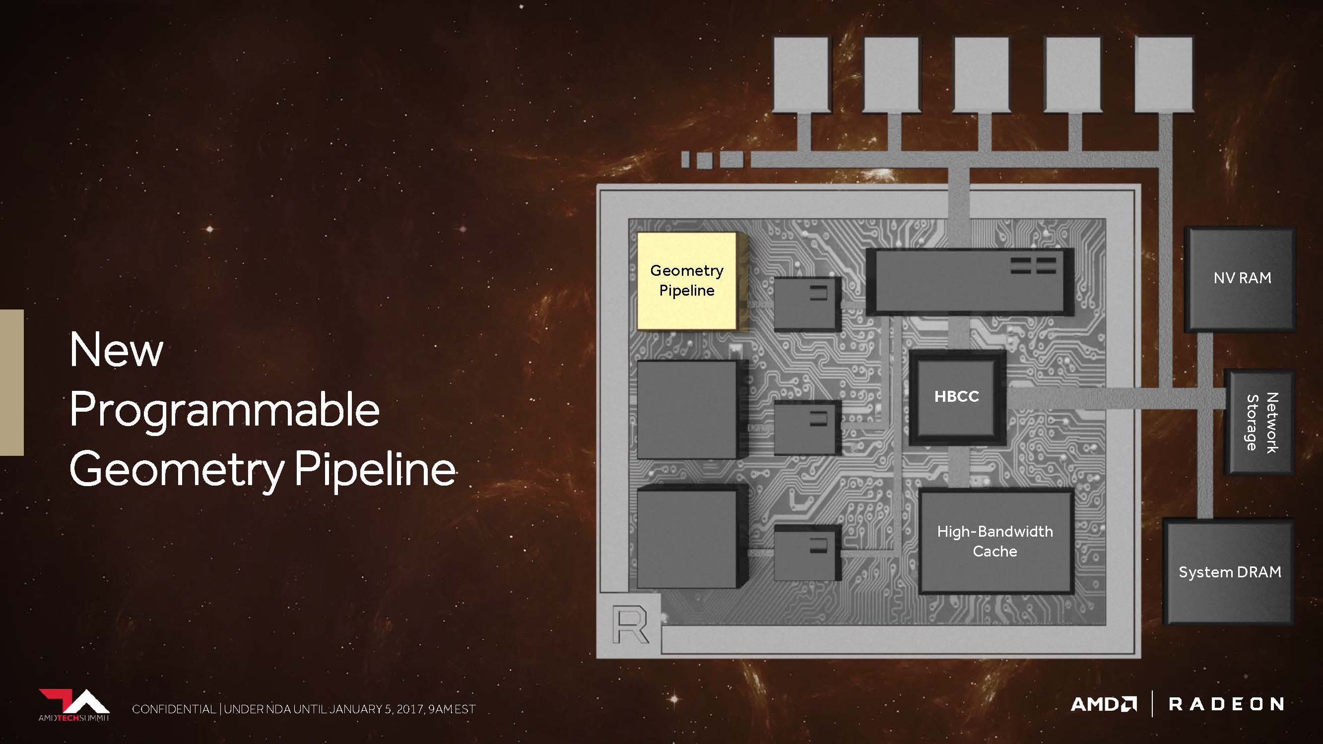
AMD's slides say that Vega should now be able to work up to 11 polygons at the top instead of the maximum four polygons per cycle, which is up to 2.75 times that. This is the result of what AMD has inserted into the geometry pipeline as the New Primitive Shader Stage. Instead of the hardware-anchored but inflexible functions, a flexible shader array is now used to process the resulting polygons.
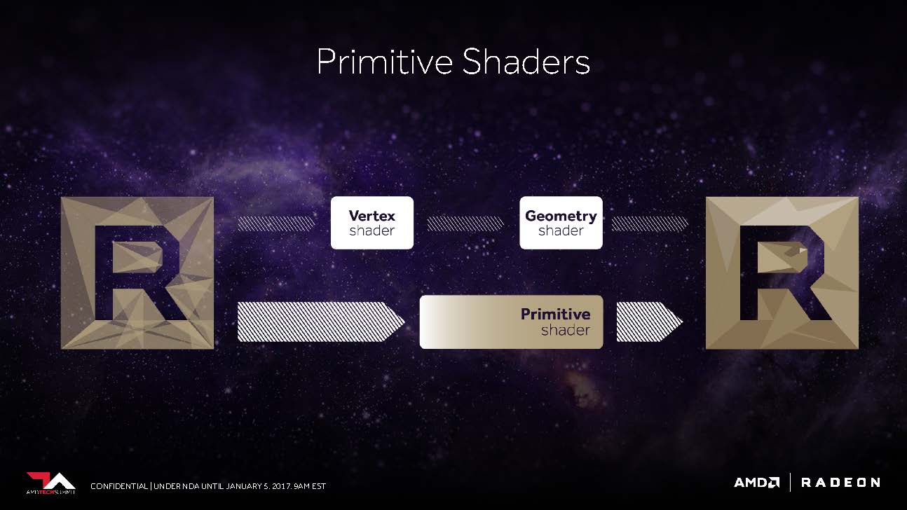
Mike Mantor, AMD Corporate Fellow, compares this to the functionality of a compute shader for processing geometry tasks – lightweight and programmable, and equipped with the ability to discard unnecessary polygons at a high rate.
AMD's Wasson also explained that this shader functionality also includes much of what DirectX offers with its vertex, envelope, domain, and geometry shader levels, but is designed to be more flexible in the order and priority of the shader. actual processing.
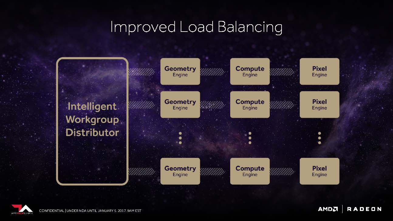
The frontend also benefits from an improved "Workgroup Distributor", which should be able to ensure the best possible load balancing around the now programmable hardware. AMD was referring to working with the efficiency-focused console developers, whose experience will now benefit PC players.
3. The Vega-NCU (Next-Generation Compute Unit)
With its Pascal-based GPUs, which are now widely represented on the market, Nvidia currently serves every segment. The largest and most expensive GP100 processor offers top FP32 power of up to 10.6 TFLOPS (at maximum boost speed). A 1:2 ratio of the FP64 cores results in peak performance with double accuracy of up to 5.3 TFLOPS. The support of FP16 (half-precision) for computing and saving allows up to 21.2 TFLOPS.
The GP102 and GP104 GPUs designed for the normal home user market still offer the equivalent FP32 performance for your shader count, but both FP64 and FP16 performance are artificially curtailed, so that these significantly cheaper maps are not very suitable for certain scientific calculations.
In contrast, it seems that AMD with Vega strives to pass on the full computing power to the end customer, even outside the MI cards presented, thus creating some added value for normal end users compared to the competitor cards.
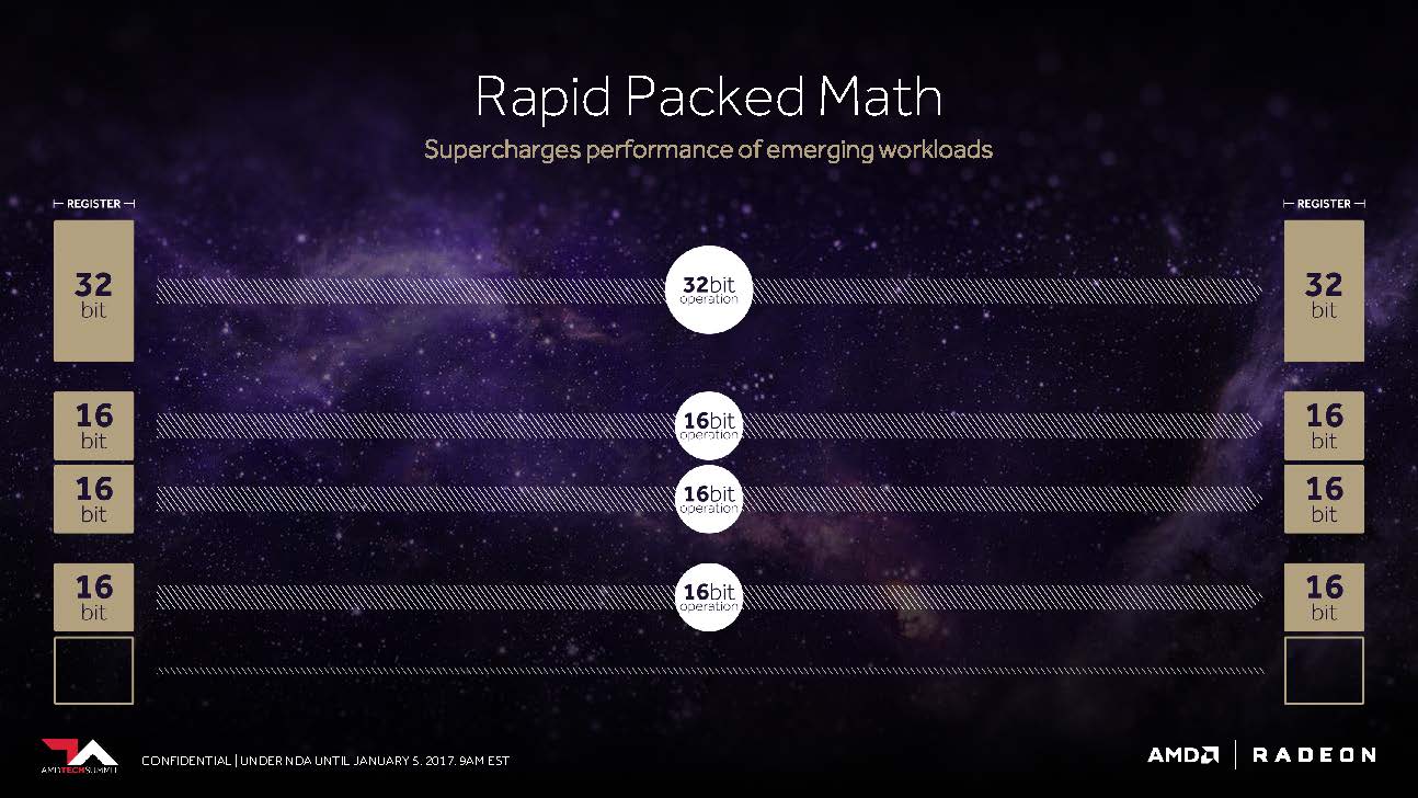
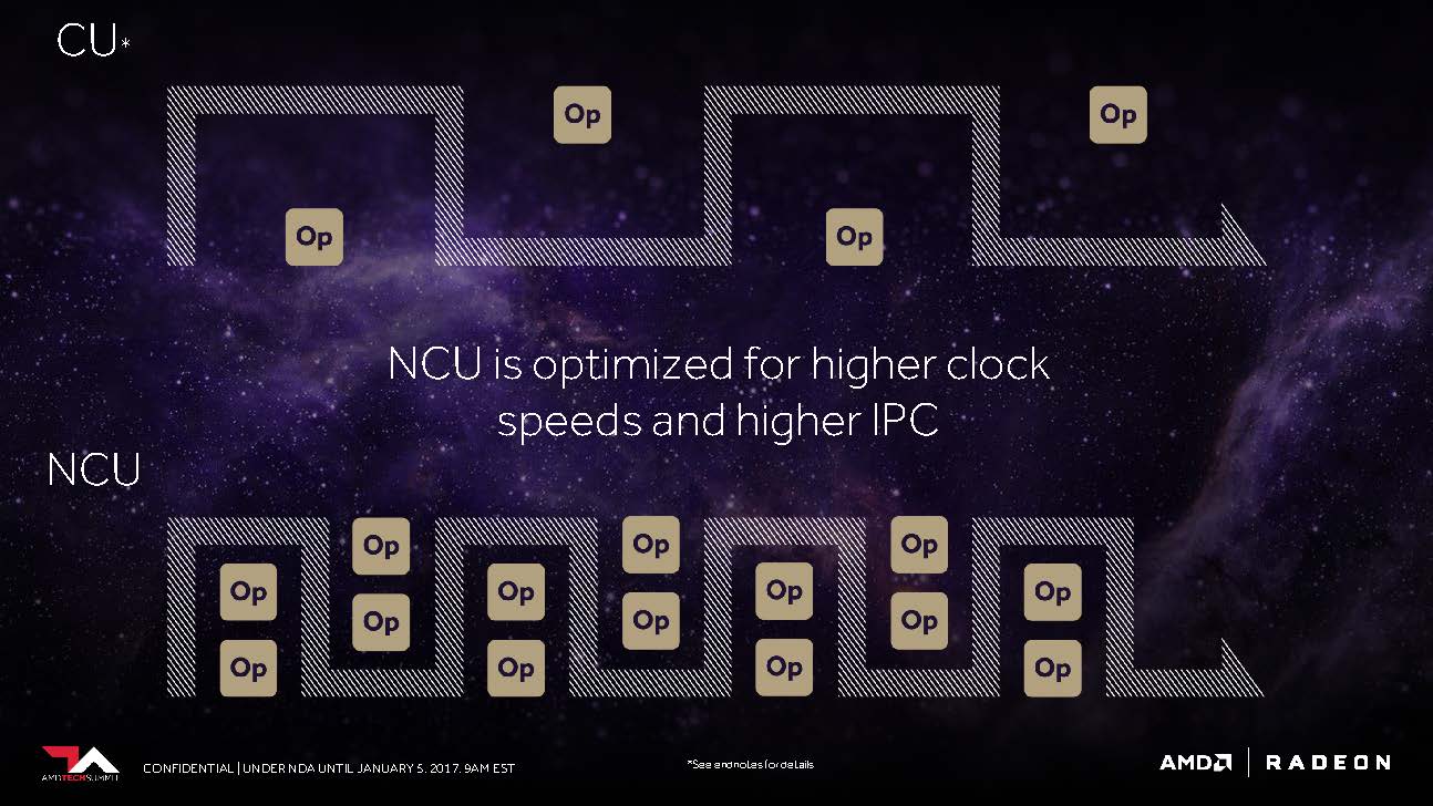
The CU block with its 64 IEEE 754-2008 compatible shaders remains as such – except that AMD now calls it NCU (Next-Generation Compute Unit), which also includes support for new data types. Logically, these 64 shaders, together with your maximum power of two floating-point operations per cycle, result in a maximum of 128 32-bit operations per cycle.
Using F16-packed calculations, this results in up to 256 16-bit operations per cycle. AMD concludes that, under optimal conditions, it could even be up to 512 8-bit operations per cycle cycle. Even with FP64 (Double Precision), AMD seems to have no problem releasing the full, uncircumcised performance to the general public.
The impetus for this flexibility may have come from the console world. After all, we know that Sony's PlayStation 4 Pro can achieve up to 8.4 TFLOPS in FP16 performance, twice its performance in 32-bit operations. Or perhaps AMD's efforts to gain a foothold in machine learning and training with products like MI25 are the real triggers.
In the end, it may even be both to poach in areas outside of Nvidia's current market presence. In both cases, new consoles, entire data centers and, of course, PC gamers as well as semi-professional users can benefit to the same extent.
AMD also said that the NCUs are optimized for higher clock rates, but this is not particularly surprising. But at the same time you also rely on larger instruction buffers in order to be able to use the computing units as well as possible over the entire time.
4th. The Next-Generation Pixel Engine
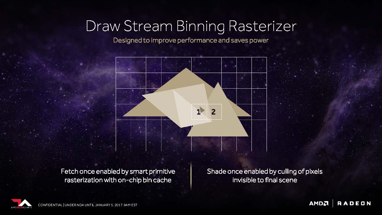
The fourth core theme in AMD's executions actually consists of two sub-areas. The first would be what Raja Koduri calls the "Draw Stream Binning Rasterizer" and which, as a complement to the traditional ROP, should be able to increase performance while still saving energy.
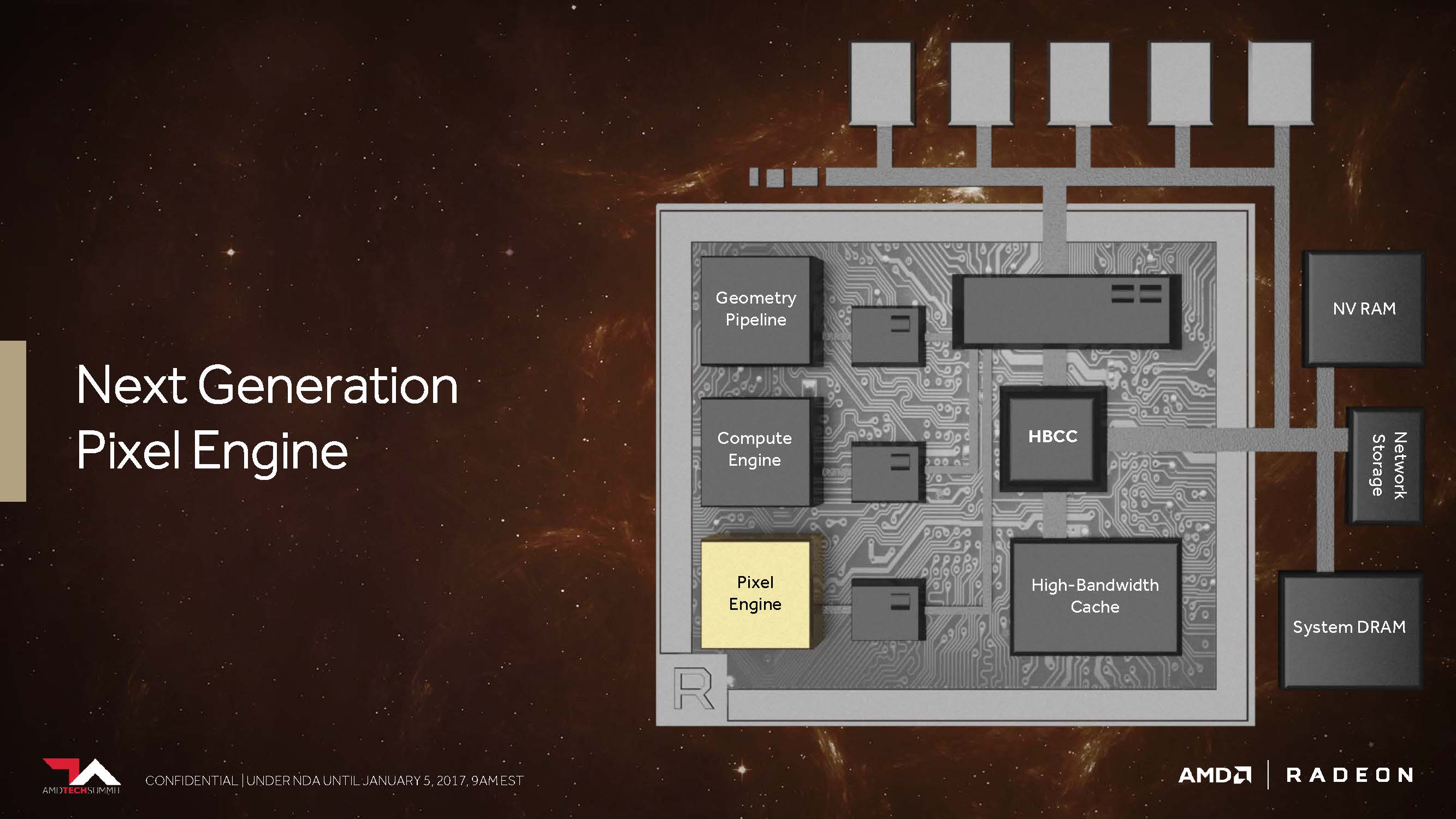
Thus, a special cache on the chip should allow the rasterizer to edit the data for intersecting polygons only once and oothe all those pixels that would not be visible in the finished scene anyway.
The second point is that AMD has changed its cache hierarchy in general and fundamentally so that the rendering backends are now directly connected to the L2 cache.
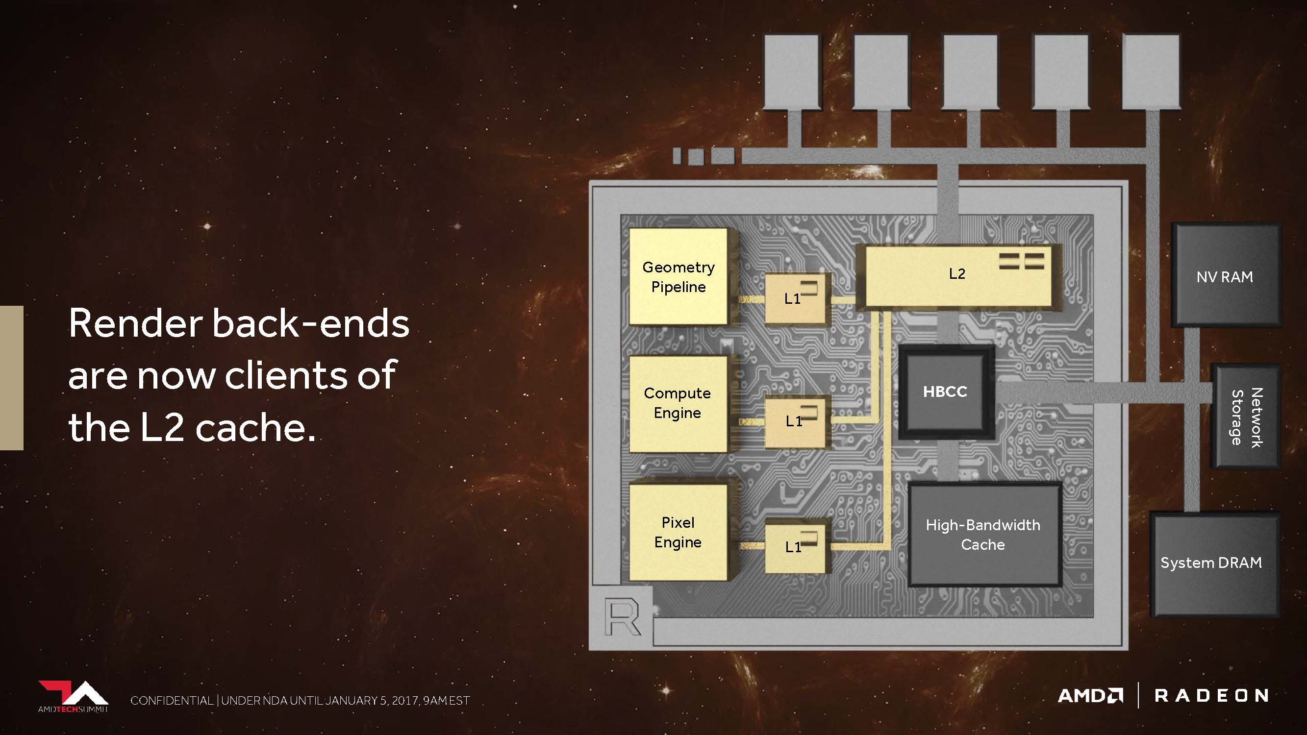
In the pre-Vega architectures, AMD did not have proper memory access for non-coherent pixels or textures that would have allowed each pipeline stage to synchronize them over a shared point.
For example, a texture rendered as a result of a scene for later use was sent all the way back to the graphics memory outside the graphics chip before it could be recalled.
AMD now bypasses this with the coherent access, which , as AMD says, should offer an enormous increase in performance whenever, for example, Deffered Shading is used.
Conclusion
The Vega chapter at the Tech Summit 2016 was a packed talk with a few real highlights and also some fillers from what we already knew.
What Raja Koduri showed us in his lecture on the new hardware will of course also require a very large development effort on the software side. In order to be able to use the new features efficiently and fully, it will probably take some time for the right adjustments.
A first glimpse of what might be possible was the Doom demonstration in Ultra HD at maximum settings, where an early Vega board could render in the playable 70 FPS range. Unfortunately, the test system was completely glued to the test system for secrecy, which also concerned the ventilation openings, so that the card, which is therefore guaranteed to work at the thermal limit, could certainly not offer the full performance.
In the end, the only conclusion left to us is the realization that everything is to be different and better, but that we have not yet been willing or willing to show more details than we have just described here. This means waiting again until real hardware, which is available for all, finally materializes from the Mira Morgana.


Kommentieren