Besonders spannend wird ein Test immer dann, wenn man dabei auf unerwartete Probleme stößt, für die das Testsubjekt eigentlich gar nicht Verantwortlich ist. So war is auch in diesem Fall. Ein RAM-Test, selbst wenn es ein eher hochpreisiges Kit ist, läuft bei mir mittlerweile nach Schema F und ist kein Hexenwerk. Aber diesmal fand ich mich in einem schon fast übernatürliche Zauber gefangen, aus dem es einen Ausweg gab: Testen, probieren und weiter tüfteln, wochenlang. Eigentlich soll es heute um die neuen Dominator Titanium RGB Module von Corsair gehen, konkret um die 2x 24 GB Variante mit einem XMP-Profil von […] (read full article...)
Du verwendest einen veralteten Browser. Es ist möglich, dass diese oder andere Internetseiten nicht korrekt angezeigt werden.
Du solltest ein Update durchführen oder einen alternativen Browser verwenden.
Du solltest ein Update durchführen oder einen alternativen Browser verwenden.
Nichts für launische Speichercontroller! – Corsair Dominator Titanium RGB DDR5-8000 2 x 24 GB Kit Review mit Teardown und Overclocking
- Themenstarter Redaktion
- Beginndatum
Veii
Veteran
- Mitglied seit
- Okt 24, 2021
- Beiträge
- 184
- Bewertungspunkte
- 212
- Punkte
- 43
If there is a situation of me misunderstanding the Review Statements , and there is no Overclocking attempts involved,
Then excuse my harsh insertion.
I got linked back here due to it spreading well.
Given longer time on this Forum and respect to Igor's hard work, including forum handling,
Plus noticing the same mistakes multiple times on multiple places. I want to finally offer an advice.
The issue in inconsistency is because:
It's all i want to comment and due to past, offer support.
Excuse me if this is taken personally, but i don't know how to tell it without hurting feelings.
May the future improve and the issue(s) in approach get noticed. For the benefit of everyone reading and our economy itself.
Thank you~
Then excuse my harsh insertion.
I got linked back here due to it spreading well.
Given longer time on this Forum and respect to Igor's hard work, including forum handling,
Plus noticing the same mistakes multiple times on multiple places. I want to finally offer an advice.
The issue in inconsistency is because:
Its unfortunate. But this blame does not belong to ASUS™. Neither to any other Boardpartners nor IC Vendors.The Board appears to lack some logic, and also expects the Overclocker/Researcher to know some logic.
If both await on the other to finish the work ~ it will sometimes train inconsistently.
It's all i want to comment and due to past, offer support.
Excuse me if this is taken personally, but i don't know how to tell it without hurting feelings.
May the future improve and the issue(s) in approach get noticed. For the benefit of everyone reading and our economy itself.
Thank you~
Zuletzt bearbeitet
:
Roland83
Urgestein
- Mitglied seit
- Okt 12, 2022
- Beiträge
- 683
- Bewertungspunkte
- 528
- Punkte
- 93
Veii
Veteran
- Mitglied seit
- Okt 24, 2021
- Beiträge
- 184
- Bewertungspunkte
- 212
- Punkte
- 43
Logical ranks exist. They have to.@Veii
1.) you have an interesting idea of ranks, especially dual rank modules.
There is no space in a 1H design per side.
Although it is a little thing to call it dual sided vs dual rank
Dual rank implies 2 commands per strobe. This is impossible without RCD who manages that.
This may be possible in a 2H UDIMM design - may, within reasons.
But this is and remains impossible with current design and anything thats out there.
Utilizing two 32bit wide links per side will not change it around. It will change writes but remain 1cmd / strobe.
Hence not dual rank but dual sided layout.
This includes access to both dimm sides given UDIMM layout. It remains 1cmd/strobe.
If in this abstract example there would be gold-fingers ontop of the dimm, and we have 4 instead two logical ranks.
It due to design will remain a 1cmd/strobe and still not be dual/quad rank.
It can not be by the definition of "dual rank" which didn't just start to exist from (G)DDR5.
If in this abstract example there would be gold-fingers ontop of the dimm, and we have 4 instead two logical ranks.
It due to design will remain a 1cmd/strobe and still not be dual/quad rank.
It can not be by the definition of "dual rank" which didn't just start to exist from (G)DDR5.
Is utilizing people's experience about "dual rank ddr4" , and marketing as such.
The 2ndary thing that slightly bothers me, but shouldn't be my worry ~ is the responsibility of target reviewer.
Because he usually explains well and does his job well.
Some voltage management issues causing him the very core trouble of this review, but that's about.
Same as the remain team over here. All work hard and do very well.
Marketing is just marketing,
But painting a reality that UDIMM can do 2 stobes per cmd, is ... i don't know how to phrase it any different than what i did.
Be it polite or impolite. It can not work.
What is done, is managing writes faster than depending on DIMM itself. Due to lets call it "abstract Arch design".
But that's it. It can not bypass the single 8nCK read-command limitation. Because its raw design doesn't allow it.
Hence it, simply calling it "dual rank" is disingenuous at best, or misleading at its core.
I think we both mutually understand the limitations of a logical rank, like the limitation of a subchannel or subgroup.
I'm sorry, but marketing with dual rank is simply wrong. Two "logical/virtual" ranks is a different topic.
DDR5 is not the first generation of multi rank layout. Changing its meaning just to suite DDR5, would be an abstract reality.
I have wrote this on post #412.) the statement told the modules want work stable or reliable using XMP profile theyre sold with on intel platforms. there was no context oc'ing it beyond that..
If i missed the intention of the review, i want to excuse myself for it.
If i understand the poking hints of "Intel MRC Lootbox" , if i may quote.
Or "ASUS's inconsistent Training" ~ which like explained, expects on the user to use logic and can correct only as much.
Then,
I honestly don't understand where i missed the point.
Given its called "XMP and OC" & was talked about the trouble of finding training stability.
Of course there is, if one see's the mentioned hints as standalone variables.
It makes sense why the supplied foundation will never be near stable. It can only correct as much.
At this point i said too much.
I can hope that we don't start to change the "dual rank" title around.
And if we are gonna go that path, might as well call our 2x 1DPC system "quad channel".
Its logical not physical , but at this point where do you even draw the line.
Just disingenuous to the users who may want to learn something. Marketing aside;
Not even hard to add a "virtual" or "logical" title before it.
Making it clear that there is no "dual rank speedup" in current UDIMM design.
Zuletzt bearbeitet
:
Veii
Veteran
- Mitglied seit
- Okt 24, 2021
- Beiträge
- 184
- Bewertungspunkte
- 212
- Punkte
- 43
At this point, we can even go down the technical path in CCD_X, S/L/M vs MR
I can not see a world where CCD_MR is being utilized in UDIMM design. Neither remain RDIMM behavior.
Because it just makes neither logical nor physical sense.
It needs to be 2H , to have any chance of functioning as " 2cmd/strobe called dual rank"
That is from the perspective of pagesize and bitwidth.
It can not function neither actively, nor in logical-layout passively, sub 1cmd per 8nCK strobe.
It feels soo adventurous that i even have to talk about it, when its soo far out of logic.
I don't know. Maybe i'm wrong;
But i'm certain that i am not. Neither subranks nor subchannels re'define physical layout limitations.
Tho marketing seems to attempt to re'define that.
It's just not dual rank & people will never have that old-experience that you try to tell them. Because it just can not work that way.
I don't know what to say more. The unfortunate thing is, that wasnt even the core reason of having to write here.
Blaming Asus or Intel due to usererrors, should have been the one and only polite hit. No further discussion neither any attacks attempted.
Lets move on~
Zuletzt bearbeitet
:
Roland83
Urgestein
- Mitglied seit
- Okt 12, 2022
- Beiträge
- 683
- Bewertungspunkte
- 528
- Punkte
- 93
That's your perspective but it's not what JEDEC classifies as a rank - but its the point ! . You can rightly think this is good or bad, but it's a fact - and it wasn't really any different looking @ DDR4.
Veii
Veteran
- Mitglied seit
- Okt 24, 2021
- Beiträge
- 184
- Bewertungspunkte
- 212
- Punkte
- 43
I really don't know how to explain you.
JEDEC may classify as Rank anything that is away of the side.
In the usual term DualSide is used.
JEDEC utilizes DS & DR
JEDEC Papers for RDIMM specify designs for DS and DR.
JEDEC Papers for UDIMM do not specify designs for DualRank.
There is a difference between Physical Rank and Logical Rank.
Its not the same thing.
Its just "DualSided" Layout with 1cmd/strobe.
And "DS" is a layout & timing name supplement, that is referenced by JC-45 & JC-45.3 Committee.
JEDEC is huge. They define targets for all sorts of flash or exotic devices. Thermal sensors and so on~
May you actually show me what you mean and teach me better ?
Because we go nowhere with this.
JEDEC may classify as Rank anything that is away of the side.
In the usual term DualSide is used.
JEDEC utilizes DS & DR
JEDEC Papers for RDIMM specify designs for DS and DR.
JEDEC Papers for UDIMM do not specify designs for DualRank.
There is a difference between Physical Rank and Logical Rank.
Its not the same thing.
There are many tCCD_X commands for distance transition states.
It defines it clearly to where it goes. Both are not the same thing.
Even Micron explains this more closely, and so also does Zentimings show you its SR not DR.
Irrelevant of logical layout or firmware/cpu based layout.
Irrelevant of FPGA layout or X86 layout.
It can be utilized many ways. LP/G/DDR5 is flexible.
On the Hardware side,
There remains a difference between Phyiscal and Logical Rank.
On the goldfingers and pinouts (check JESD308A , JESD309-S4 & JESD305-R8)
There is a difference and its stated.
That UDIMM can not utilize 2cmd/strobe is not book-theory but facts.
Irrelevant how you design your architecture around it.
What "i" think doesn't matter here.
To make a Phyical Rank that acts as such and can jump between 2 commands/strobe state (one at a time),
you need VDDQ line to be able to be isolated from either (H)eight location. Hence 2H designs exist.
There is no passthrough VIA between pads of each IC , between sides.
Its all roundtrip & consumers don't utilize neither 2H nor 4H or any other exotic 3DS designs, for this to be a thing.
It physically can not exist nor function. This includes how its called on Firmware level.
Firmware doesn't call it physical rank either. It needs to isolate a rank completely.
Memory is not quantum either. It has one state per time, due to the usage of discharging capacitors
as 1Transistor1Capacitor "Cell". It can not have more than those states in their current form
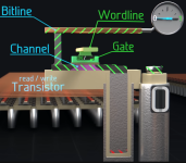
To make "dual rank" aka 2cmd/strobe, you need a switching line and a 2nd line !
This switching is handled by RCD-IC.
IC-Passthrough through PCB is not a thing.
It physically can not do the things you tell me it should do , to deserve "Dual Rank" title.
It defines it clearly to where it goes. Both are not the same thing.
Even Micron explains this more closely, and so also does Zentimings show you its SR not DR.
Irrelevant of logical layout or firmware/cpu based layout.
Irrelevant of FPGA layout or X86 layout.
It can be utilized many ways. LP/G/DDR5 is flexible.
On the Hardware side,
There remains a difference between Phyiscal and Logical Rank.
On the goldfingers and pinouts (check JESD308A , JESD309-S4 & JESD305-R8)
There is a difference and its stated.
That UDIMM can not utilize 2cmd/strobe is not book-theory but facts.
Irrelevant how you design your architecture around it.
What "i" think doesn't matter here.
To make a Phyical Rank that acts as such and can jump between 2 commands/strobe state (one at a time),
you need VDDQ line to be able to be isolated from either (H)eight location. Hence 2H designs exist.
There is no passthrough VIA between pads of each IC , between sides.
Its all roundtrip & consumers don't utilize neither 2H nor 4H or any other exotic 3DS designs, for this to be a thing.
It physically can not exist nor function. This includes how its called on Firmware level.
Firmware doesn't call it physical rank either. It needs to isolate a rank completely.
Memory is not quantum either. It has one state per time, due to the usage of discharging capacitors
as 1Transistor1Capacitor "Cell". It can not have more than those states in their current form

To make "dual rank" aka 2cmd/strobe, you need a switching line and a 2nd line !
This switching is handled by RCD-IC.
IC-Passthrough through PCB is not a thing.
It physically can not do the things you tell me it should do , to deserve "Dual Rank" title.
And "DS" is a layout & timing name supplement, that is referenced by JC-45 & JC-45.3 Committee.
JEDEC is huge. They define targets for all sorts of flash or exotic devices. Thermal sensors and so on~
May you actually show me what you mean and teach me better ?
Because we go nowhere with this.
Zuletzt bearbeitet
:
Veii
Veteran
- Mitglied seit
- Okt 24, 2021
- Beiträge
- 184
- Bewertungspunkte
- 212
- Punkte
- 43
Lets think further:
If you can follow my "theory" of how UDIMM can become Dual Rank
And we use actually Committee's words for this
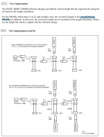
There are drafts how to make a 2H UDIMM.
But ...
Like mentioned,
You need this:
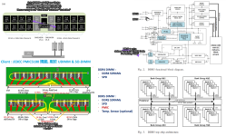
^ borrowing a pic from another topic of mine
A 2 height layout, that allows CS_ to switch between both Subchannel_A 4 ICs + Subchannel_B 4 ICs ~ as one VDDQ line.
And switch to the remain diagonal SubchannelA_01 with SubchannelB_00 together.
Then ! you can do 2 cmd's per strobe and interleave between ranks. Alternating between both states. Top & Bottom ICs.
The rest as you can also see on the edited picture, are logical ranks ~ which DO NOT have passthrough VIA's through the PCB.
This is the 3rd time i'm repeating this.
Without this, while DQ's may be able to be targeted , there remains one VDDQ.
You have no way to push through to the other side, and just use delayed DS roundtrip commands.
Its not within the same strobe. It is close to indifferentiable vs a read to read with 8nCK delay. (between Bankgroups)
It is not a 4nCK read. Only RDIMM can do that. A real symmetrical 2H Dual-Rank does do this, 2 commands per 8nck strobe.
A QuadRank is then 4H , tho i can not imagine how 4H 3DS would even look like. Cube design? but how.
A 2H UDIMM does not exist in the current state. It could exist based on comitee's UDIMM definitions, but they do not exist.
Soo no, it is not DualRank and also no, it will not be able to get the processing speedup that we know from DDR4.
It just can not. There is no reason to continue using the term wrongly and so confuse users in buying FairyTales.
Please show me something that i have missed and you try to explain.
I'm human and make mistakes or miss a point. I'm open to listen and learn.
But at "this point" , you are just being undeniably inoperable in accepting information which conflicts with whatever you have read online.
This is incorrect.
I own most of the papers and watched multiple seminars.
This statement is incorrect.
There is a clear description what a single & multi-rank design looks like.
"Dual/QuadRank" title is a consumer shortening. DualSided is equally such but used in FW.
MixedRank is the command name next to DualSided.
DR naming is used on Intel's FW, but its for different rank, not dual rank.
Mixed Rank management & link assignment happens through standalone RCD_IC, not through timings !
Please be reasonable.
Also after LPDDR4, DDR5 is such a leap and milestone in design.
It is completely different than DDR4. While it is close to LPDDR4, which is vastly different from DDR4
It is non-comparable to DDR4. Neither in Firmware, nor in Design;
Maybe it can be compared to GDDR5 to 5X, given its scale'ability and adaptiveness to different layout-factors. Its logical and physical differentiations.
But no.
If you can follow my "theory" of how UDIMM can become Dual Rank
And we use actually Committee's words for this

There are drafts how to make a 2H UDIMM.
But ...
Like mentioned,
You need this:

^ borrowing a pic from another topic of mine
A 2 height layout, that allows CS_ to switch between both Subchannel_A 4 ICs + Subchannel_B 4 ICs ~ as one VDDQ line.
And switch to the remain diagonal SubchannelA_01 with SubchannelB_00 together.
Then ! you can do 2 cmd's per strobe and interleave between ranks. Alternating between both states. Top & Bottom ICs.
The rest as you can also see on the edited picture, are logical ranks ~ which DO NOT have passthrough VIA's through the PCB.
This is the 3rd time i'm repeating this.
Without this, while DQ's may be able to be targeted , there remains one VDDQ.
You have no way to push through to the other side, and just use delayed DS roundtrip commands.
Its not within the same strobe. It is close to indifferentiable vs a read to read with 8nCK delay. (between Bankgroups)
It is not a 4nCK read. Only RDIMM can do that. A real symmetrical 2H Dual-Rank does do this, 2 commands per 8nck strobe.
A QuadRank is then 4H , tho i can not imagine how 4H 3DS would even look like. Cube design? but how.
A 2H UDIMM does not exist in the current state. It could exist based on comitee's UDIMM definitions, but they do not exist.
Soo no, it is not DualRank and also no, it will not be able to get the processing speedup that we know from DDR4.
It just can not. There is no reason to continue using the term wrongly and so confuse users in buying FairyTales.
Please show me something that i have missed and you try to explain.
I'm human and make mistakes or miss a point. I'm open to listen and learn.
But at "this point" , you are just being undeniably inoperable in accepting information which conflicts with whatever you have read online.
No.not what JEDEC classifies as a rank
it wasn't really any different looking @ DDR4
This is incorrect.
I own most of the papers and watched multiple seminars.
This statement is incorrect.
There is a clear description what a single & multi-rank design looks like.
"Dual/QuadRank" title is a consumer shortening. DualSided is equally such but used in FW.
MixedRank is the command name next to DualSided.
DR naming is used on Intel's FW, but its for different rank, not dual rank.
Mixed Rank management & link assignment happens through standalone RCD_IC, not through timings !
Please be reasonable.
Also after LPDDR4, DDR5 is such a leap and milestone in design.
It is completely different than DDR4. While it is close to LPDDR4, which is vastly different from DDR4
It is non-comparable to DDR4. Neither in Firmware, nor in Design;
Maybe it can be compared to GDDR5 to 5X, given its scale'ability and adaptiveness to different layout-factors. Its logical and physical differentiations.
But no.
Zuletzt bearbeitet
:
skullbringer
Veteran
- Mitglied seit
- Sep 14, 2020
- Beiträge
- 306
- Bewertungspunkte
- 328
- Punkte
- 64
@Veii Sorry, you talk too much and say too little. I can't follow you at all, maybe I'm too stupid.
1. "Ranks":
If you have 128 bits of connectors on a 64 bit wide bus, that's dual rank as far as I know. That's simply what happens when you put 16 pieces of x8 wide memory ICs on a memory PCB.
If that is not correct, please link the source.
2. "VREF"
Explain what to set and why, and I will try. I've been doing DDR5 overclocking since it came to market and this experience is the base of reviews like this one. Of course, I cannot say for sure, that there isn't some secret to DDR5 overclocking, just that I haven't found such a secret in like 2 years.
And even if there is such a secret like VREF tuning, that I'm simply missing out on, 1. why is this not communicated better in forums and by vendors? and 2. why is there not better optimization in place after such a long time that DDR5 has been available for mainstream?
Apart from all that, arguing about such a secret is only valid for manual memory overclocking, not XMP/EXPO. XMP/EXPO is supposed to be plug and play, that's the whole idea behind it. If any setting required to stabilize the XMP/EXPO kit is not in the profile or automatically set, it's not suitable for XMP/EXPO operation. Simple as that.
Roland83
Urgestein
- Mitglied seit
- Okt 12, 2022
- Beiträge
- 683
- Bewertungspunkte
- 528
- Punkte
- 93
Ich glaube er vermischt da vieles aus dem Bereich Registered und unregistered über die techn Unterschiede bei DDR4/5 hinweg und ohne einen wirklichen Zusammenhang. Es stimmt manches im einzelnen was er da von sich gibt - hat aber oft im Zusammenhang nichts miteinander zu tun, oder ich kann seinen Argumenten einfach nicht folgen…, und eigentlich auch schon gar nicht mit Gamer PC Dimms oder deren OC..
8j0ern
Urgestein
- Mitglied seit
- Mrz 4, 2021
- Beiträge
- 2.515
- Bewertungspunkte
- 790
- Punkte
- 113
Hello, as I know about Dual-Rank DIMM is, this is the Internal Organisation of the RAM Modul.
With AMD IMC you have a wider Data-Bus to improve Bandwidth at the same clocks.
That result in a higher RAM Bandwidth as Single-Rank.
With AMD IMC you have a wider Data-Bus to improve Bandwidth at the same clocks.
That result in a higher RAM Bandwidth as Single-Rank.
