


Before we get to overclocking the modules, I first need to say a few words about my test systems. Since Intel Rocket Lake was recently released and the platform made a notable gain in memory performance, I replaced the 10900KF previously used for testing with a 11700K. Of course, this means that performance and OC results should not be directly compared between tests with these different CPUs. While the 10900KF could still be operated stably at well over 5 GHz, the 11700K already reaches its limits at around this barrier. The results in benchmarks, which primarily scale with the CPU clock, are correspondingly lower.
So the 11700K is run with the default boost and power limits lifted. Only the cache was manually increased to 4.4 GHz to minimize the bottleneck towards the memory controller as much as possible. As in past tests, a single-ranked Samsung B-Die kit from G.Skill serves as the control kit, in order to be able to rank today’s test kit relative to it in the market. The AMD test system uses a 5950X with maximum PBO on a Gigabyte B550 Aorus Pro v2, which is ideal for RAM overclocking due to its optimized DIMM slot topology. The following is a summary of the information on the test systems:
| Test systems | |
|---|---|
| Hardware: |
Intel platform
AMD platform
|
| Cooling: |
|
| Housing: |
|
| Periphery: |
|
The modules are tested on both platforms with 3 settings each: 1. XMP, 2. with a simple overclock where only the clock speed is raised, and 3. a maximum performance and voltage setting with completely manually set secondary and tertiary timings. While the clock rate on the Intel platform can also be increased further in the Gear 2 with correspondingly relaxed timings, the performance on the AMD platform suffers too much from the 1:2 gear ratio. Therefore, instead of higher clock speeds, tighter timings are used here for maximum performance. The overclocks were also tested for stability with Testmem5 v0.12 and the profile “Anta777@Extreme1”, just like in the heatsink stress test.
Overclocking the Talos modules from today’s test turned out to be relatively pleasant, as a setting either ended in BSOD after 2 minutes in the stress test or was completely stable. The fact that single errors creep in after several minutes or hours only happens if the RAM voltage is raised above 1.45V. For example, I can’t stabilize DDR4-4533 with 1.5 V even with extremely loose primary timings. The ICs of this memory kit don’t seem to like voltages above 1.45V at all. But be it as it may, because even with this limitation considerable benchmark results can be achieved for a RAM kit in this class, but more about that on the next page.
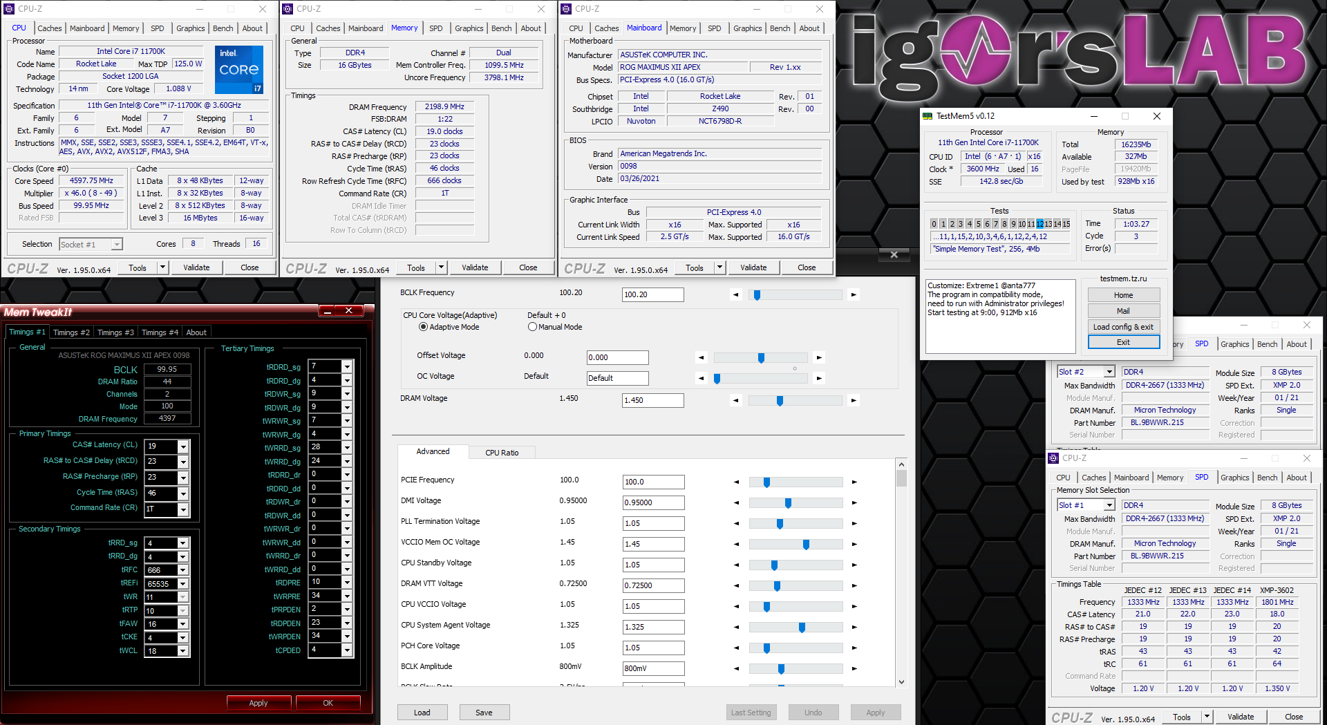
On the Intel platform the maximum stable clock rate is DDR4-4400 with primary timings 19-23-23-46, of course in Gear 2 and thus an effective memory controller clock rate of 1100 MHz. With these memory ICs, tRCD did not scale with the RAM voltage, such as with Samsung 8 Gbit B-Die and in general, as I said, we have relatively little freedom with the voltage. In return, however, tCL can be tightened considerably relative to the clock rate, so that there is a small gain in access latency. While tRFC can only be set to 666 and thus not much lower than auto, the remaining secondary timings can be tightened relatively strongly.
For tary timings, tRDRD_sg and tWRWR_sg cannot be lowered from the auto value of 7. However, with the tRDWR timings of 9, you can get a decent increase in bandwidth and also save some latency gains with the tWRRD timings of 24 and 28. In addition to the RAM voltage, 1.3 V System Agent and 1.45 V VCCIO Mem voltages are used for this setting.
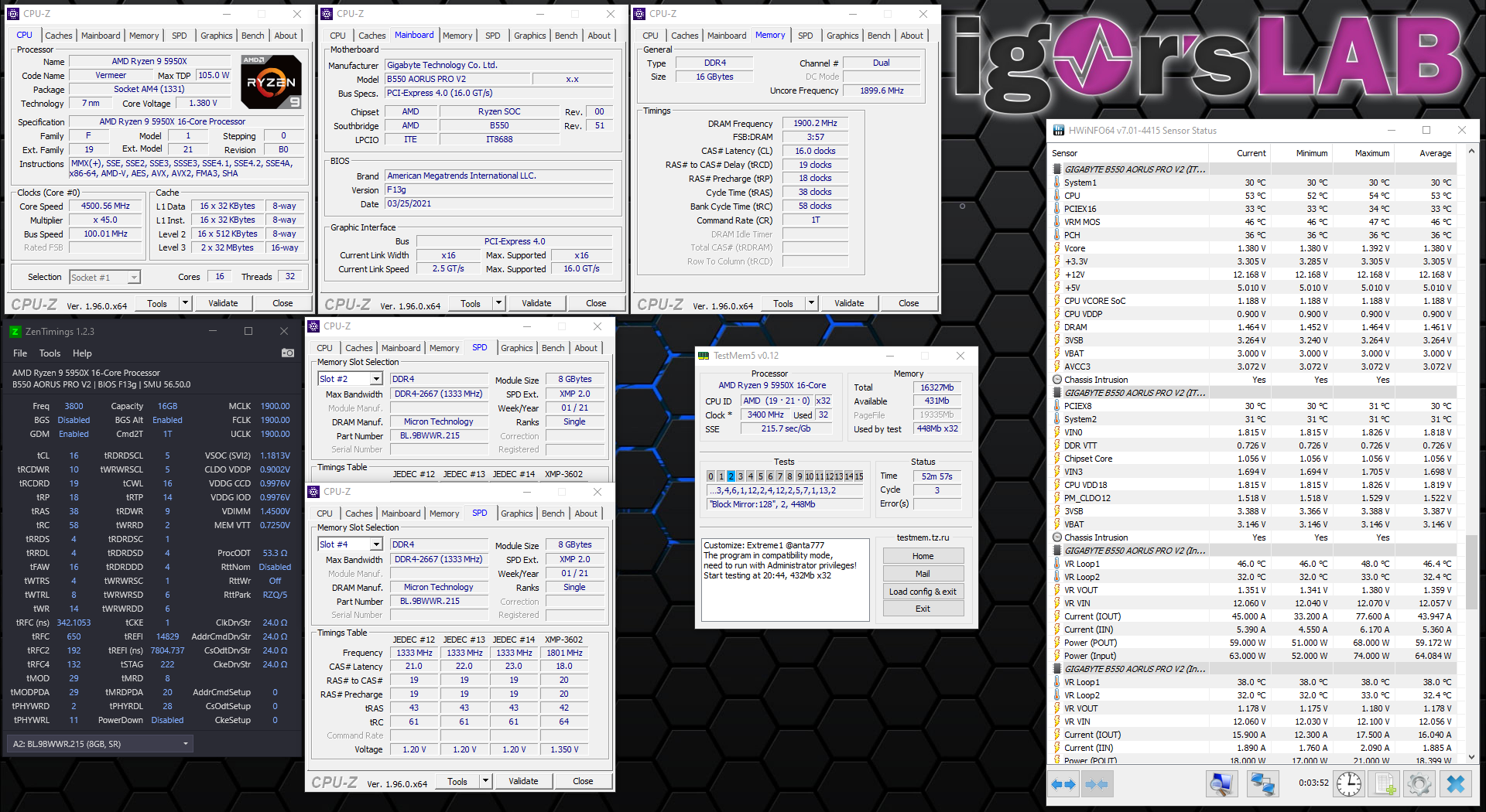
On the AMD platform, as mentioned, we are limited by the maximum Infinity Fabric clock of the CPU, which is 1900 MHz, and thus to an effective RAM clock rate of DDR4-3800 in 1:1 mode. By increasing the RAM voltage to 1.45 V, however, the timings can be lowered here instead of a higher clock and thus latency above all can be gained. The only truly performance-critical timings that cannot be changed from their Auto value are tRDRDSCL and tWRWRSCL with 5. One can see a parallel to the tRDRD_sg and tWRWR_sg setting on the Intel platform.Here, besides the voltage for the RAM, no others need to be adjusted, since the memory ICs do not represent a large load for the memory controller.
So what are these pseudo Micron ICs with 8 Gbit capacity that don’t like more than 1.45 V voltage, but can still be clocked relatively high? Since Micron currently only produces 8 Gbit Rev E and 16 Gbit Rev B in the DDR4 consumer area, the selection here is relatively small. The clock performance would also fit RevE, as you can also see in my very first review on igorslab of the Crucial Ballistix 3200 CL16 kit. Now the only question is why these Micron ICs don’t have Micron laser engraving on them? This is also relatively easy to explain if one remembers that BIWIN also masters chip packaging and can process Micron wafers into “own” memory chips. So the ICs used in this kit will most likely be Micron RevE in the BIWIN package.


6 Antworten
Kommentar
Lade neue Kommentare
Urgestein
Urgestein
Urgestein
Urgestein
Veteran
Urgestein
Alle Kommentare lesen unter igor´sLAB Community →