Board layout
The Vega64 and Vega Frontier Edition have the same board, 100% identical components and differ only by the soldered package with the halved memory expansion, as well as a customized firmware. The length, if you look at the right side of the PCB, is only due to the radiator structure with the large radial fan. By a sensible shortening, it would be easy to achieve board sizes in the format of an R9 Nano.
AMD has therefore thought a bit about the division of the board, especially since the elimination of the external memory modules opens up new possibilities. Exactly in their place you now place the individual power supplies. We see an almost classic 6+1 phase design for GPU and memory, as well as other voltage converters for the respective partial voltages. We will go into all these things in more detail, because it is really interesting.
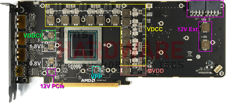
The two 8-pin connectors are each connected via a coil, which helps to smooth certain voltage peaks. However, we could not find larger capacitors here.
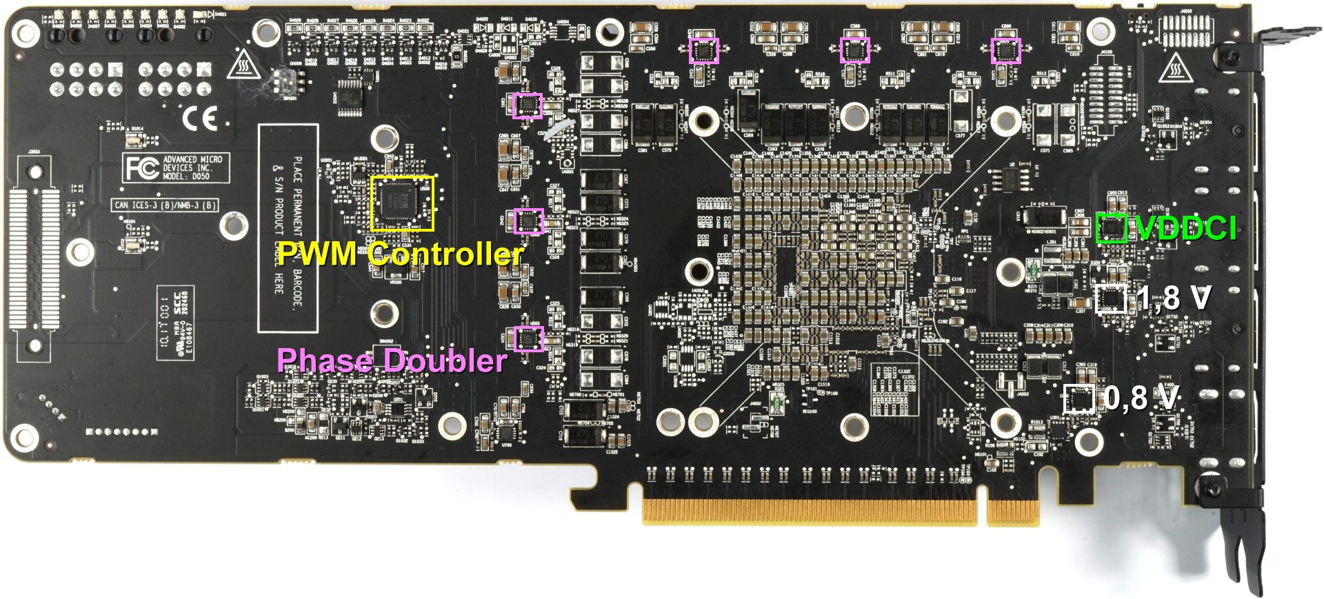
On the back, besides the very tightly equipped base of the package, we see the PWM controller as the most obvious part, as well as other components whose positioning we should remember, because we want to show a video right away.
Power supply of the GPU
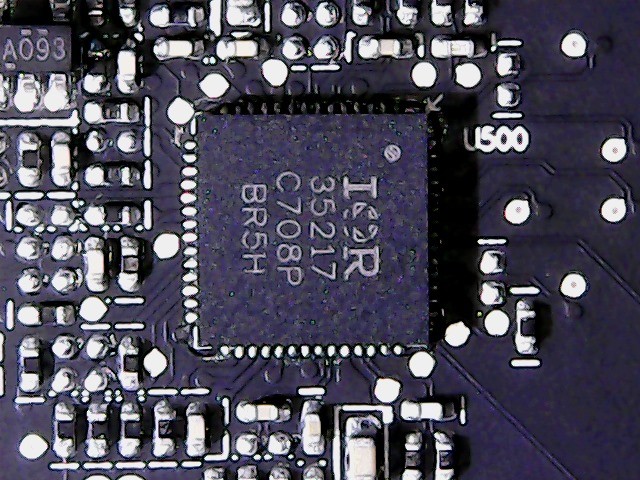
First of all, the focus is on the IR3521 from International Rectifier, a dual output digital multi-phase controller that can provide both the 6 phases for the GPU and 2 other phases, which we will talk about in a moment. But back to the GPU. After all, we count twelve voltage transformer circuits, not six. However, since only six real phases can be created, you can double each of these phases in order to divide the load into two converter circles. We suspect that this effort will not be done later with the slightly simpler XL version. for this, you either simply owe away the space for the second circle or simplify the board as such.
 |
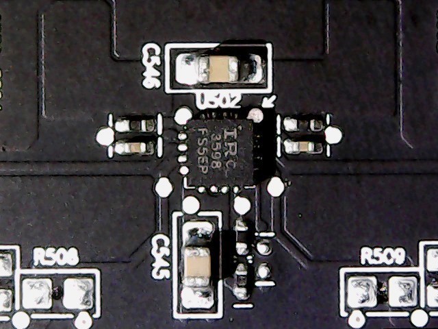 |
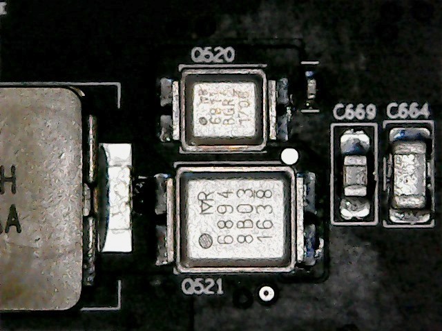
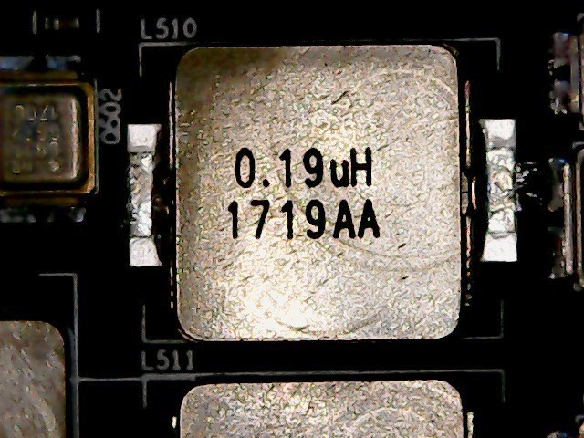
A total of six IR3598s are used for this so-called doubling, which are located on the back of the board (we remember). The actual voltage conversion of each of the twelve converter circuits is performed by an IRF6811 on the high side and an IRF6894 on the low-side, which also contains the required Schottky diode. Both are previously USED by AMD HEXFETs from International Rectifier. In the case of coils, AMD relies on encapsulated and front-soldered ferrite core coils. The inductance is slightly lower at 190 nH than the usual 220 nH for THE GPUs.
 |
 |
Power supply of the memory
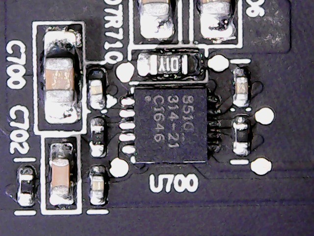
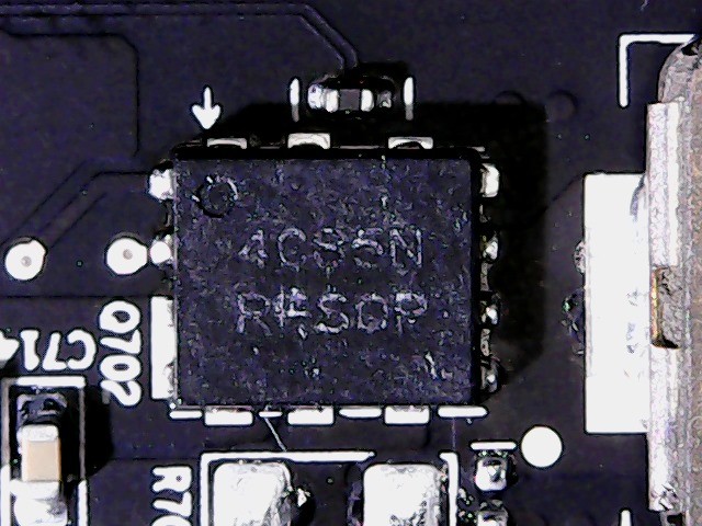
As mentioned briefly, the IR35217 also provides one phase for storage. One phase is sufficient because the memory is much more adequate. The gate-driver CHL815 is back on the back of the board, while an NTMFD 4C85M from ON Semiconductor is used for voltage conversion. This dual N-Channel MOSFET realizes both the high and the low-side.
 |
 |
It is also interesting that AMD generally dispenses with all cup capacitors and only relies on flat SMD caps. The slightly lower capacity can be compensated by simply switching two of these caps in parallel and usually also using the back of the board. A sensible equalization of the thermal hotspots and a larger heat dissipation also have the nice side effect that you can also enter a temperature class lower and thus also save costs. The finance department is certainly equally pleased with this.
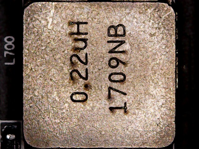
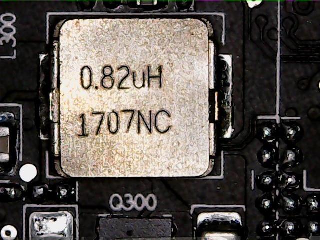
The coil is slightly larger this time with 220 nH. At 820 nH, on the other hand, the coils for the significantly slower clocking converters of the other partial voltages are even larger, which, however, also have to withstand significantly lower currents.
 |
 |
Other voltage converters
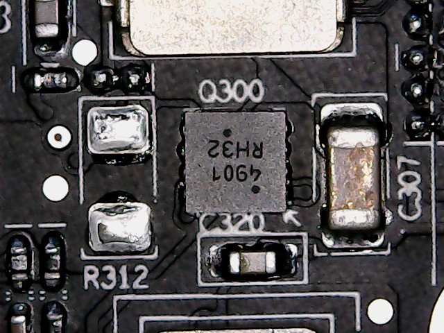
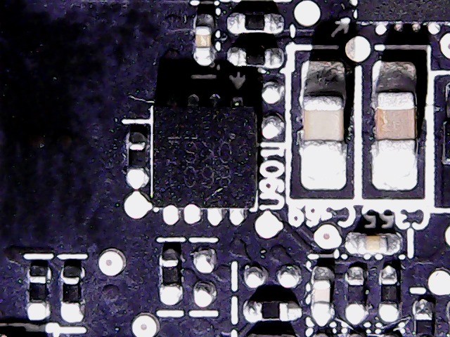
The production of VDDCI is not a big item in terms of performance, but it is important. It is used for GPU-internal level transition between the GPU and memory signals, something like the voltage between the memory and the GPU core on the I/O bus. In addition, two constant sources for 1.8V and 0.8 volts are produced.
 |
 |
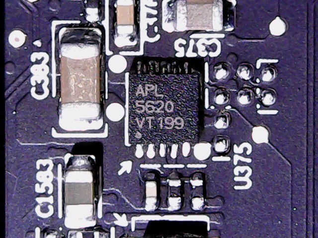
Below the GPU you can also find the APL5620 from Anpec for the VPP. This ultra-low dropout chip generates the very low voltage for the Phase Locked Loop (PLL) range.
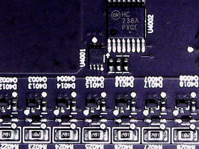
With the HC238A from ON Semiconductor as a de-multiplexer, the "mausekino" is realized for the LED bar, which shows the utilization of the power supply. Nice gimmick, but in intensity almost disturbing. Especially at night.
 |
 |
That would be the way we got through, because the rest is the usual standard.
- 1 - Einführung und Übersicht
- 2 - Details zu Architektur und HBM2-Speicher
- 3 - Demontage, Kühler und Interposer-Details
- 4 - Platinendesign und Detailinformationen
- 5 - Ashes of the Singularity: Escalation
- 6 - Battlefield 1
- 7 - Warhammer 40,000: Dawn of War III
- 8 - Doom (2016)
- 9 - Tom Clancy's Ghost Recon Wildlands
- 10 - Hitman (2016)
- 11 - Metro Last Light (Redux)
- 12 - Rise of the Tomb Raider
- 13 - Tom Clancy's The Division
- 14 - The Witcher 3
- 15 - Und kann sie Mining?
- 16 - Leistungsaufnahme im Detail
- 17 - Takt, Temperaturen und Geräuschemission
- 18 - Zusammenfassung und Fazit








Kommentieren