


Also at the risk of us repeating ourselves, we want to go back to the most important innovations at Vega. With the Vega64, AMD is now offering a new generation of GPUs after the Vega Frontier Edition, which is said to have undergone over 200 changes and improvements in the redesign of the architecture. Even if in the end it probably boils down to a kind of new GCN generation: AMD emphasized once again that this is a completely new solution.

HBM2 as a scalable storage architecture
AmD's first indication of Vegas' architectural change is the storage and the entire associated infrastructure. The reason for this focus is the ever-increasing memory requirement. Both AMD and Nvidia work separately on ways to reduce host processor overhead, maximize throughput, minimizing bottlenecks in accessing the GPU, especially those that are data sets can occur again and again.
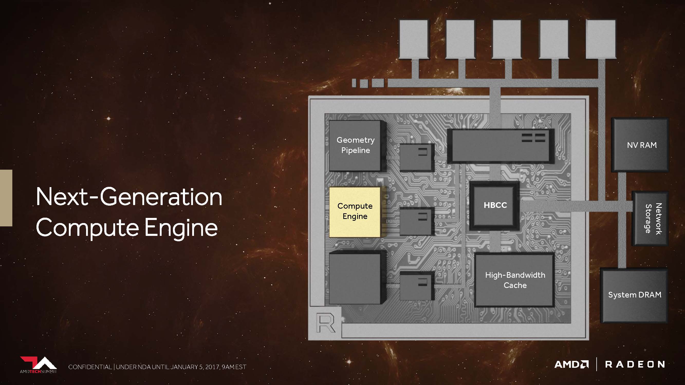
It is therefore important to bring even more memory capacities even closer to the GPU and not to let the costs explode. It seems that AMD Vega has moved a big step closer to this important goal with a much more flexible storage hierarchy. With HBM2, Vega uses an interesting new component for this, and this collection of on-package storage, which was once quite unspectacularly called a frame buffer, is now brilliantly called the "High Bandwidth Cache".
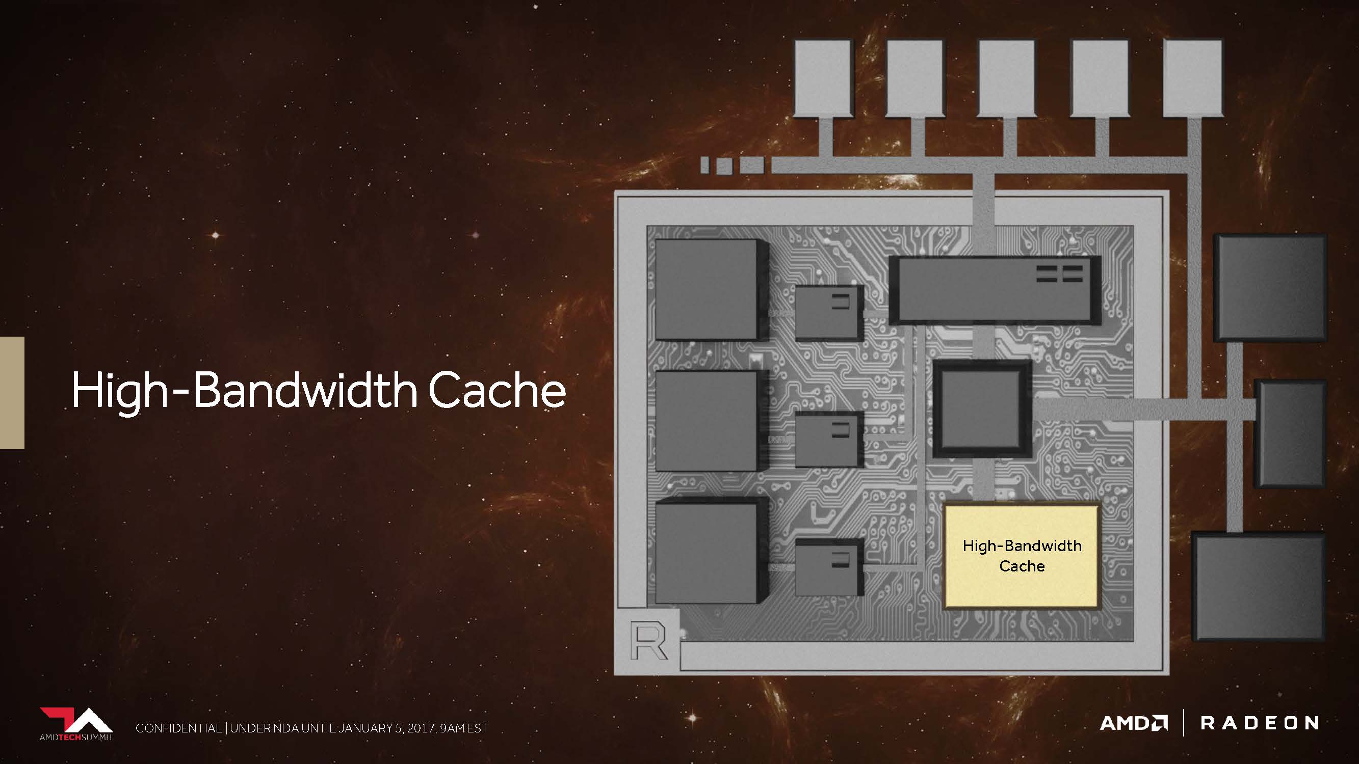
Already at HBM (and Fiji), AMD had the vision to bring the most powerful memory as close as possible to the GPU. This also includes the working and data storage of the entire system. And even if this includes significantly slower technologies in this infrastructure, HBM2 should be seen as a consistent continuation of the path taken. After all, an up to eight-fold increase in the capacity of each stack in direct comparison to the first generation is quite a considerable step forward, especially since doubling the bandwidth per pin also helps to significantly increase the maximum possible throughput of the whole.
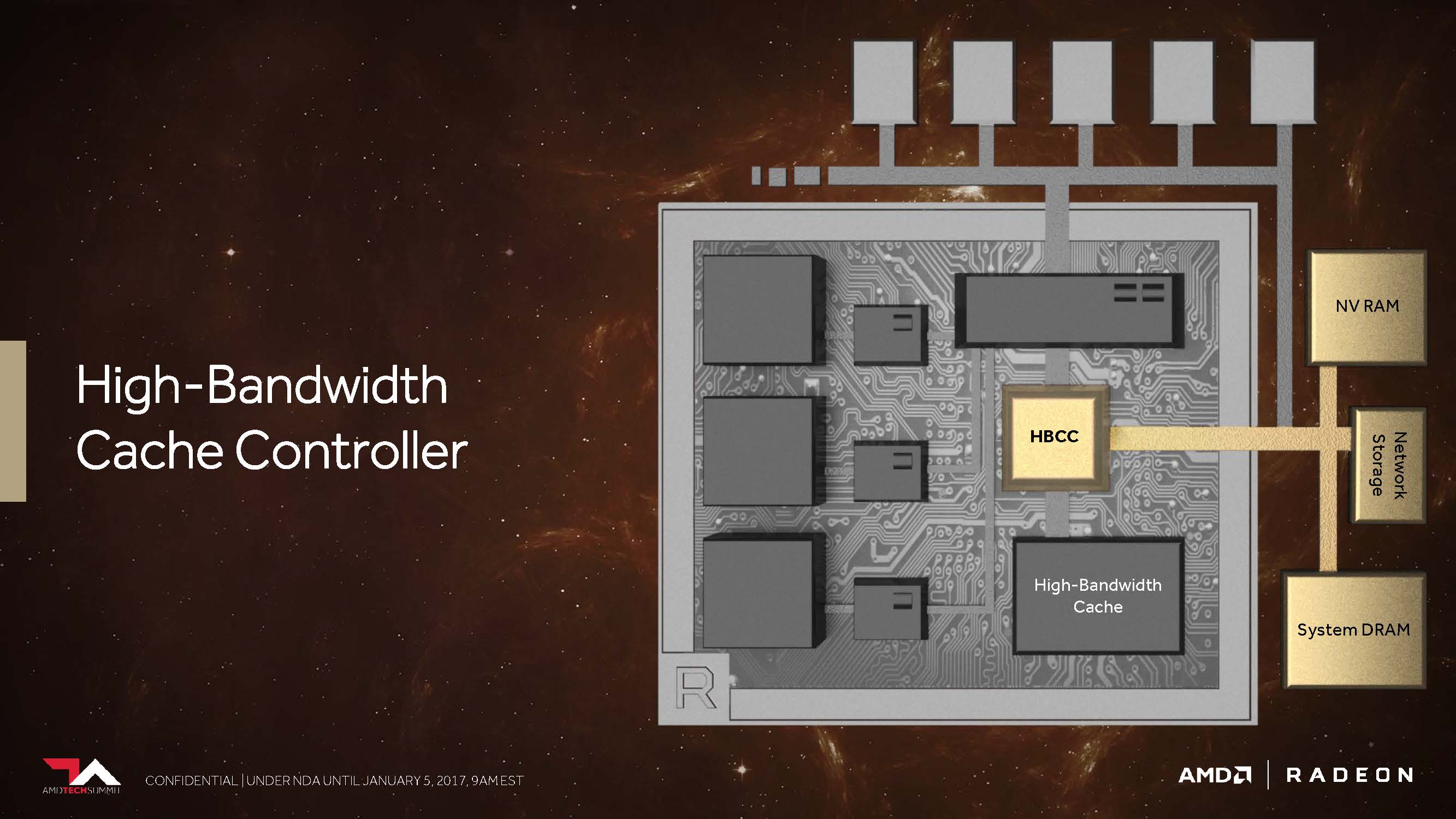
This could have the biggest impact on gaming performance if it relates to the actual storage subsystem. AMD also gives the new "High Bandwidth Cache" controller (HBCC), which has to perform more than the previous storage controller, at least virtually addressable 512 terabytes for extremely large amounts of data. Of course, you only have to use it. However, thanks to HBCC, Vega is able to move memory pages even more finely, using various programmable techniques. Thus, a received data request can be realized asynchronously via the DMA transfer, while the GPU has already switched to another thread in order to be able to continue working there without interruption.
This means that the controller actually receives the data "on-demand", but it can also return it in a forward-looking manner. In addition, information stored in the HBM in system memory can be easily replicated like an additional cache, or the HBCC – which seems even more important – can do with a single instance in order to save space and reduce overhead.
New programmable geometry pipeline
Let's just remember: The first HawaiiGPU on the Radeon R9 290 X brought some notable improvements compared to the Tahiti GPU on the Radeon HD 7970. One of them concerned an improved front end with now four instead of two geometry units, each of which each had a Geometry assembler, a Vertex assembler, and a tessellation unit.
The subsequent Fiji GPU as Radeon R9 Fury X then again relied on this already known hawaiian configuration, but brought with it some other innovations – for example, a significantly increased tessellation performance. Currently, the Ellesmere GPU (Radeon RX 480) uses a new handful of techniques to use the same constellation with the four geometry units through various filter algorithms or discarding unnecessary polygons to provide a performance benefit.
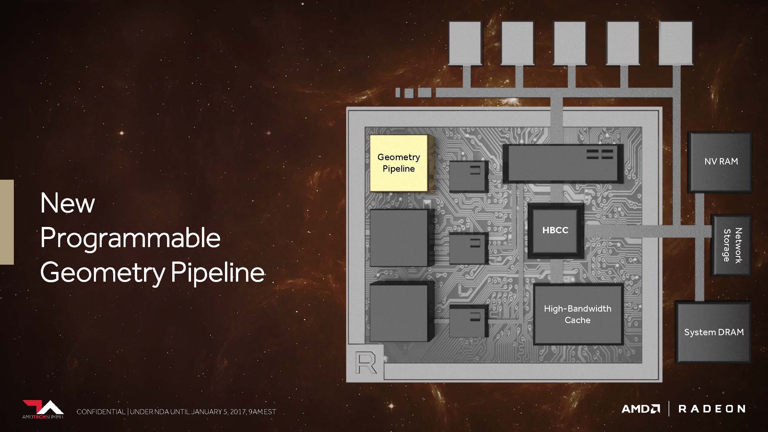
AMD promised us last year that Vega would now be able to work up to 11 polygons at the top instead of the maximum four polygons per cycle, which is up to 2.75 times that. This is the result of what AMD has inserted into the geometry pipeline as the New Primitive Shader Stage. Instead of the hardware-anchored but inflexible functions, a flexible shader array is now used to process the resulting polygons.
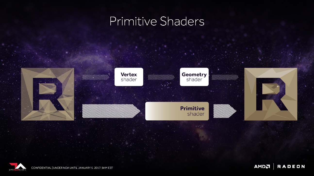
This can best be compared with the functionality of a compute shader for processing the geometry tasks – easy and programmable, and equipped with the ability to discard unnecessary polygons at a high rate. Of course, this shader functionality also contains much of what DirectX offers with its vertex, envelope, domain, and geometry shader levels, but you want to be more flexible in the order and priority of the actual processing.
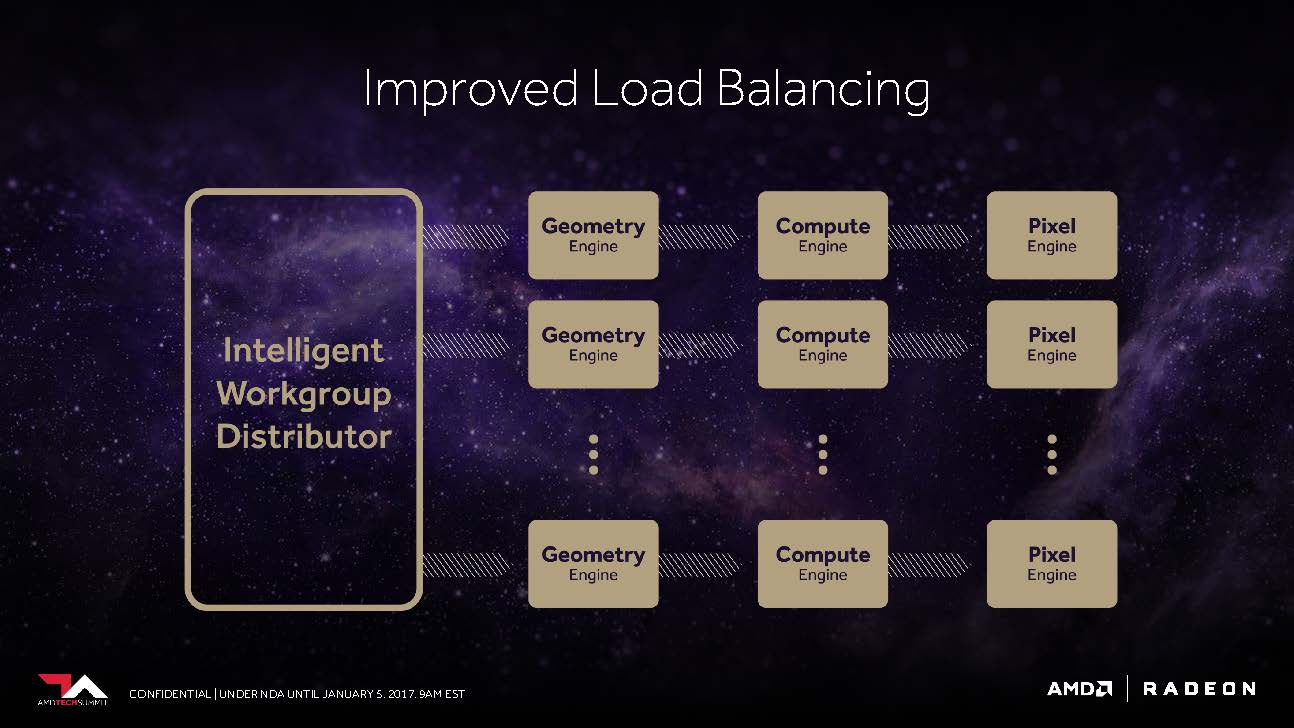
The frontend also benefits from an improved "Workgroup Distributor", which should be able to ensure the best possible load balancing around the now programmable hardware.
The Vega-NCU (Next-Generation Compute Unit)
With its Pascal-based GPUs, which are now widely represented on the market, Nvidia currently serves every segment. The largest and most expensive GP100 processor offers top FP32 power of up to 10.6 TFLOPS (at maximum boost speed). A 1:2 ratio of the FP64 cores results in peak performance with double accuracy of up to 5.3 TFLOPS. The support of FP16 (half-precision) for computing and saving allows up to 21.2 TFLOPS.
Designed for the normal home user market, the GP102 and GP104 GPUs still offer the equivalent FP32 performance for your shader count, but both FP64 and FP16 performance are artificially curtailed, making them significantly cheaper maps are not very suitable for certain scientific calculations.
In contrast, with Vega and frontier edition in particular, AMD strives to pass on the full computing power to the end customer, even outside the MI cards presented, thus providing some added value for normal end users compared to the competitor cards. Create. At least as a marketing approach, this even makes sense, because you are sure to reach a completely new target group with it.
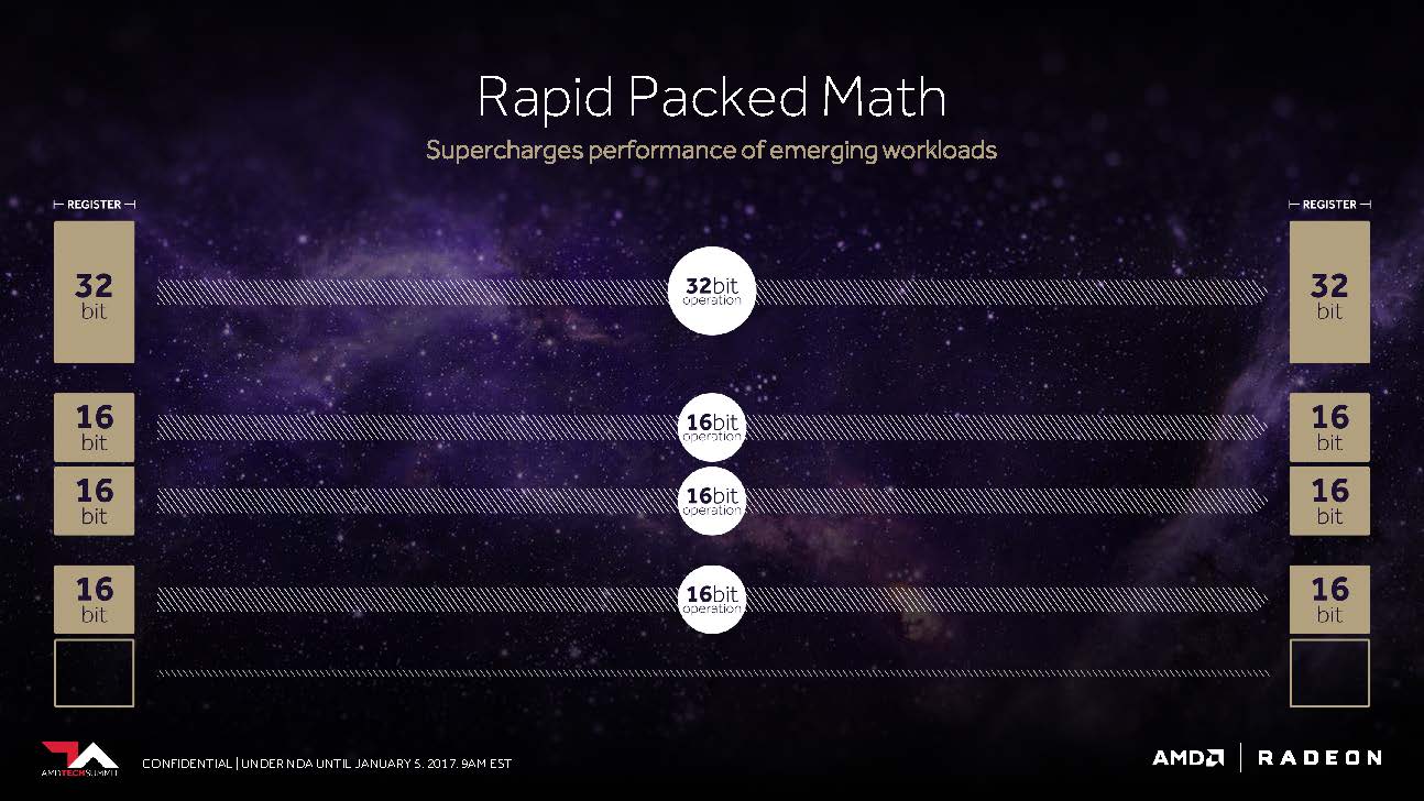
The CU block with its 64 IEEE 754-2008 compatible shaders remains as such – only that AMD now calls it NCU (Next-Generation Compute Unit), which also includes support for new data types. Logically, these 64 shaders, together with your maximum power of two floating-point operations per cycle, result in a maximum of 128 32-bit operations per cycle.
Using F16-packed calculations, this results in up to 256 16-bit operations per cycle. AMD concludes that, under optimal conditions, it could even be up to 512 8-bit operations per cycle cycle. Even with FP64 (Double Precision), AMD seems to have no problem releasing the full, uncircumcised performance to the general public.
The impetus for this flexibility may have come from the console world. After all, we know that Sony's PlayStation 4 Pro can achieve up to 8.4 TFLOPS in FP16 performance, twice its performance in 32-bit operations. Or perhaps AMD's efforts to gain a foothold in machine learning and training with products like MI25 are the real triggers.
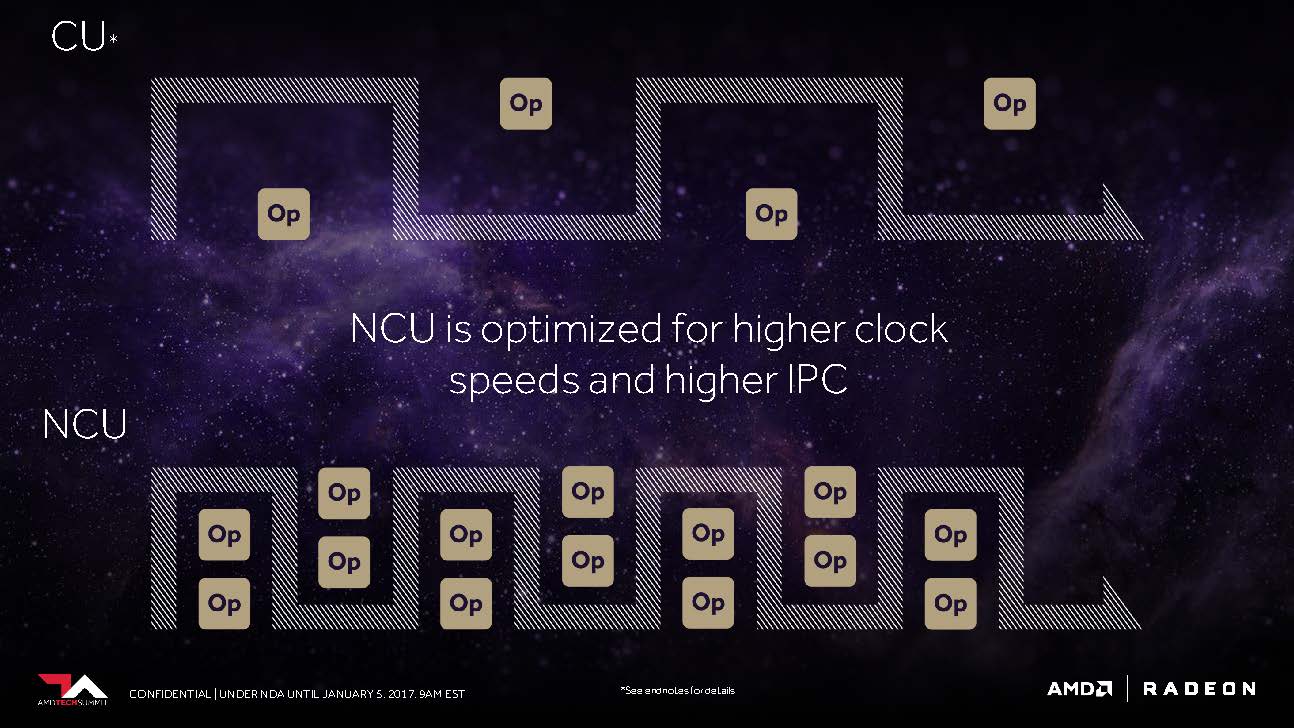
In the end, it may even be both to poach in areas outside of Nvidia's current market presence. In both cases, new consoles, entire data centers and, of course, PC gamers as well as semi-professional users can benefit to the same extent. In addition to the fact that the NCUs have also been optimized for higher clock rates, it also relies on larger instruction buffers in order to be able to use the computing units as well as possible over the entire time.
Next-Generation Pixel Engine and a Question Mark
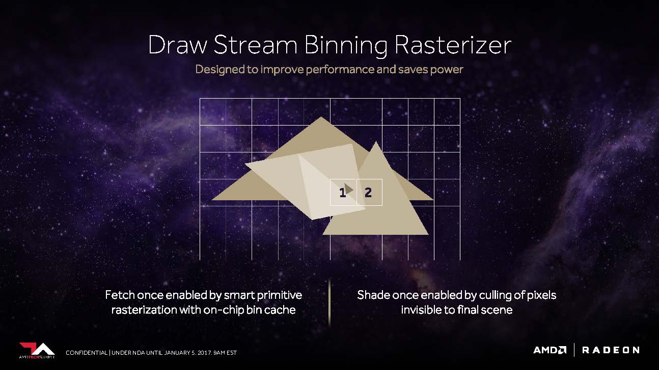
Let's move on to what AMD calls the "Draw Stream Binning Rasterizer," which, as a complement to the traditional ROP, should be able to improve performance while also saving energy.
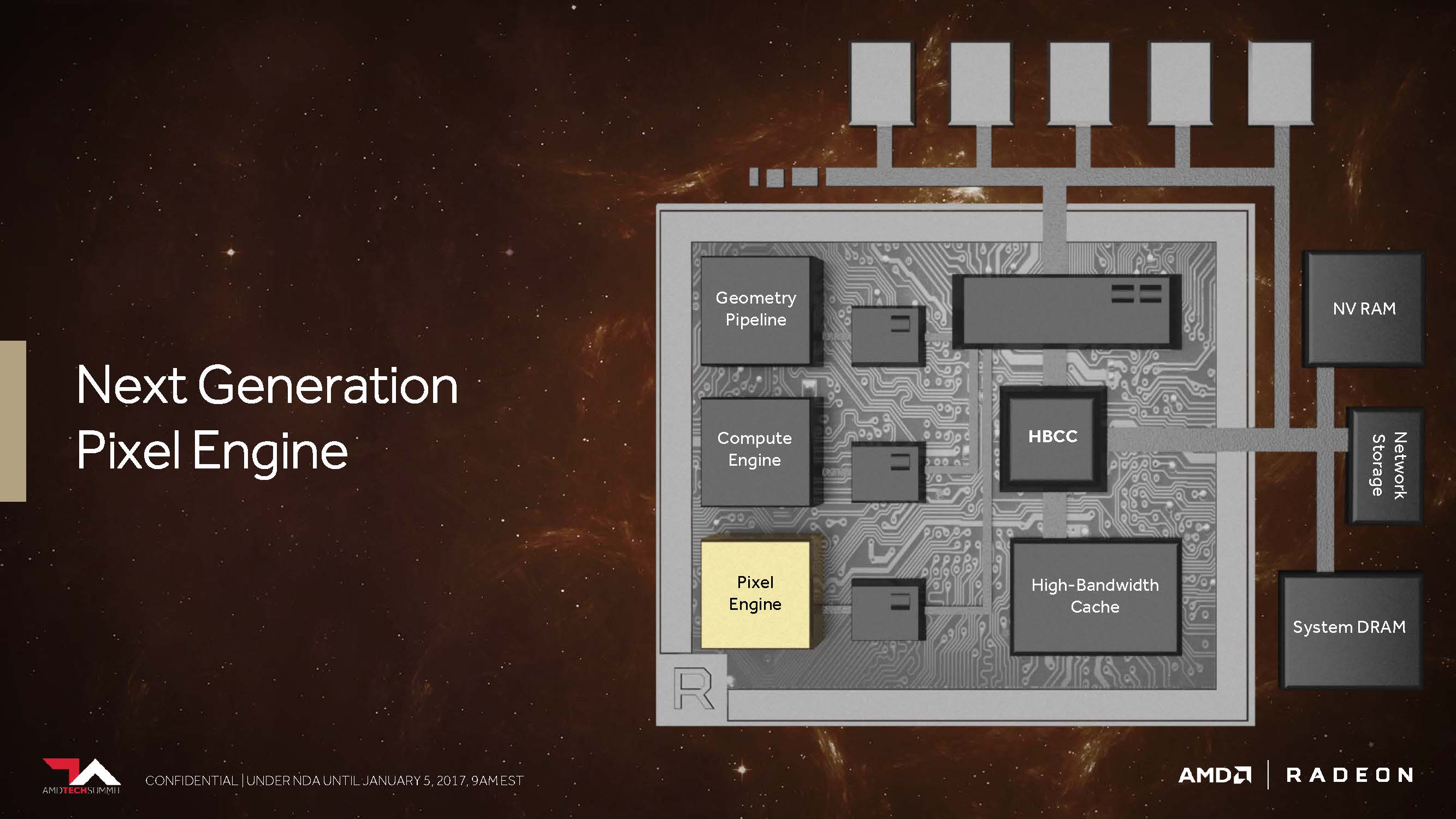
Thus, a special cache on the chip should allow the rasterizer to edit the data for intersecting polygons only once and oothe all those pixels that would not be visible in the finished scene anyway.
The second point is that AMD has changed its cache hierarchy in general and fundamentally so that the rendering backends are now directly connected to the L2 cache.
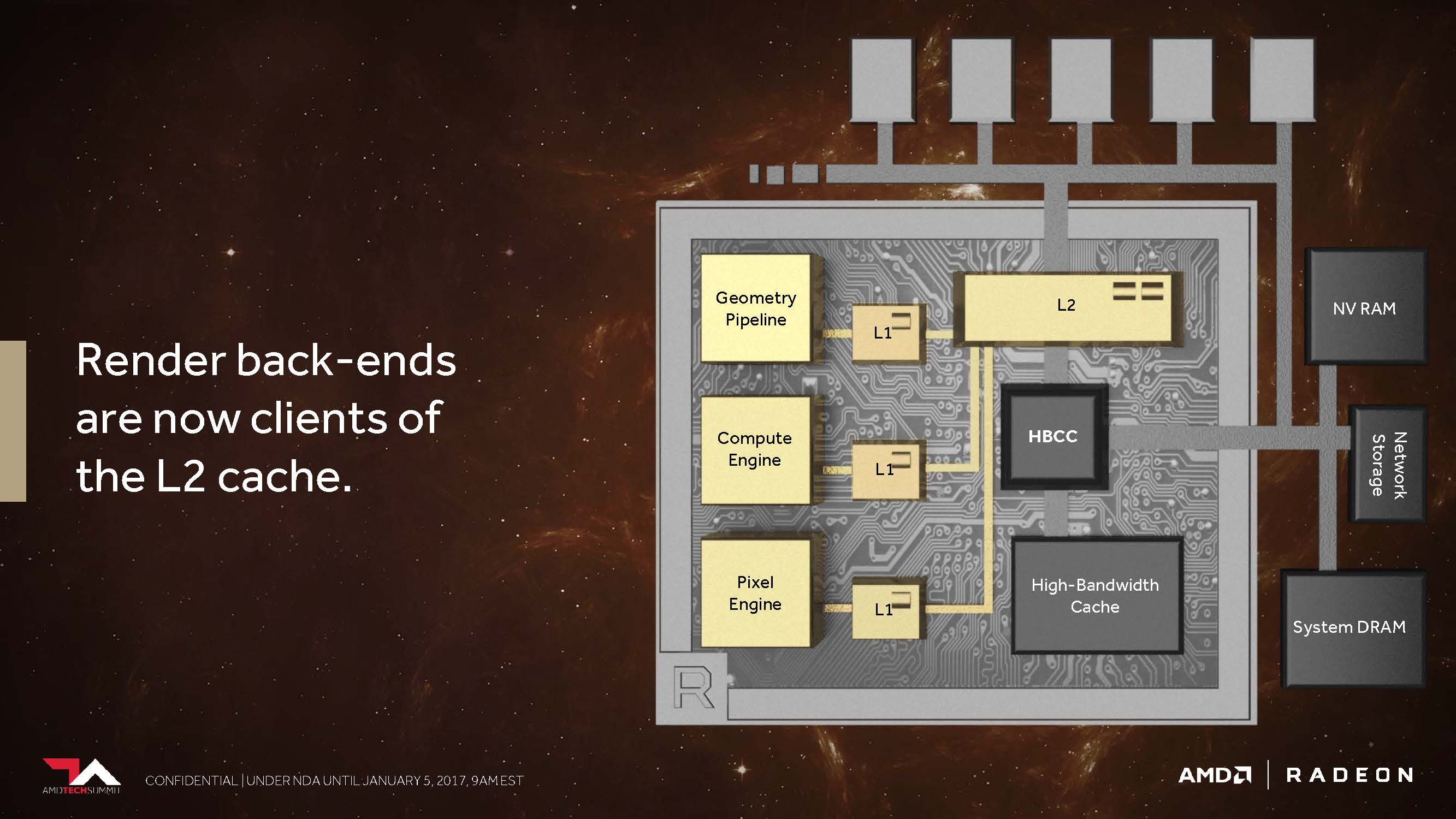
In the pre-Vega architectures, AMD did not have proper memory access for non-coherent pixels or textures that would have allowed each pipeline stage to synchronize them over a shared point. For example, a texture rendered as a result of a scene for later use was sent all the way back to the graphics memory outside the graphics chip before it could be recalled. AMD now handles all of this with the coherent access, which , as AMD says, should offer an enormous increase in performance whenever, for example, Deffered Shading is used.
But – without wanting to spoil in detail now – this promised rocket has not yet been able to ignite even with the use of the latest driver. BIOS update, drivers or nothing – everything is certainly still possible over time. And so it will probably amount to what was already the case with Fiji and Hawaii – good wine has to ripen first (especially red). But a sensation? Let's wait for the benchmarks of the next pages.
- 1 - Einführung und Übersicht
- 2 - Details zu Architektur und HBM2-Speicher
- 3 - Demontage, Kühler und Interposer-Details
- 4 - Platinendesign und Detailinformationen
- 5 - Ashes of the Singularity: Escalation
- 6 - Battlefield 1
- 7 - Warhammer 40,000: Dawn of War III
- 8 - Doom (2016)
- 9 - Tom Clancy's Ghost Recon Wildlands
- 10 - Hitman (2016)
- 11 - Metro Last Light (Redux)
- 12 - Rise of the Tomb Raider
- 13 - Tom Clancy's The Division
- 14 - The Witcher 3
- 15 - Und kann sie Mining?
- 16 - Leistungsaufnahme im Detail
- 17 - Takt, Temperaturen und Geräuschemission
- 18 - Zusammenfassung und Fazit


Kommentieren