


Various binnings in NVIDIA’s GeForce RTX 4070 – MSRP cards with unintended OC feature and the technical background (of Boost) | Exclusive
Binning as pre-selection and the role of “Speedo”
So, now comes the threatened theory, but I want to keep it as simple as possible and also explain the most important terms to you right away. First, let’s stay quite general. The so-called binning refers to the sorting of GPUs into different quality classes (“buckets”) within a certain from-to range. The individual GPUs from such a “bucket” can therefore also deviate from each other and from each other once again, but only within the framework of the specified tolerances (so-called “GPU lottery” at the customer).
When one purchases a graphics card, they may be products with differently advertised clock speeds, but they all have the same design and manufacturing process. However, the GPUs are separated from each other due to process variation (quality variation). However, they all have something in common: a maximum power specification known as TGP (aka Total GPU Power). With which I would like to remind you of the inversion of this fact with the MSRP cards on page one, which also has something to do with “Virtual Binning”.
This is then namely next higher step. Here one generally puts together different buckets with identical clock rates. However, the AIC and the end customer always place the greatest value on the ratio of performance to required energy, so NVIDIA therefore offers the buyers “buckets” that only include chips that also offer the same performance with similar TGP. That can be more frugal or thirstier, but within the bucket all GPUs are at least more or less equally fast. The only difference between the “buckets” is the different power consumption.
These “buckets” can then be operated at very different voltages, depending on the quality level. The power specification is the maximum of a virtual performance of such a “bucket”. The actual implementation, in the final consequence, is then solely to run slower chips at higher voltages and faster chips at lower voltages to achieve the best performance for a given power environment. The chip’s clock speed (slow vs. fast) is controlled by a variable called “Speedo”, which is baked into the GPU during the ATE flow as part of the FT (Final Test) phase.
Right now, though, I think I need to explain a few things. ATE stands for “Automated Test Equipment.” These are systems that automatically test electronic components or printed circuit boards for functionality and quality (to increase production efficiency and reduce defect rates). The “Final Test Phase” is the last test phase in a production or development process where all previously identified defects are corrected and the product is tested for functionality, performance and quality.
“Speedo” is a term used in the semiconductor industry for circuits that monitor process, voltage and temperature (PVT) variations in integrated circuits. Such specialized Speedo circuits allow GPUs to dynamically adjust their performance and power consumption by accounting for the chips’ response to changes in process, voltage, and temperature. These adjustments can be achieved, for example, by changing the clock frequency and supply voltage. I’ll get to that in the very next paragraph.
The telemetry of current NVIDIA graphics cards
Now I want to describe NVIDIA’s Boost (and in a coarser form also AMD’s Power Tune) and put what I just read into a more general context, even though I’m sure I’ll have to repeat myself a bit (scheme below). The task of the so-called telemetry is to achieve the maximum graphics performance with the minimum possible power consumption and the resulting side effects, such as waste heat, and to use all the monitoring data for this. The main concern is to adjust the GPU’s core voltage in real time as much as possible so that only as much power is supplied as is actually needed for the GPU’s current workload and reaching the optimal clock rate.
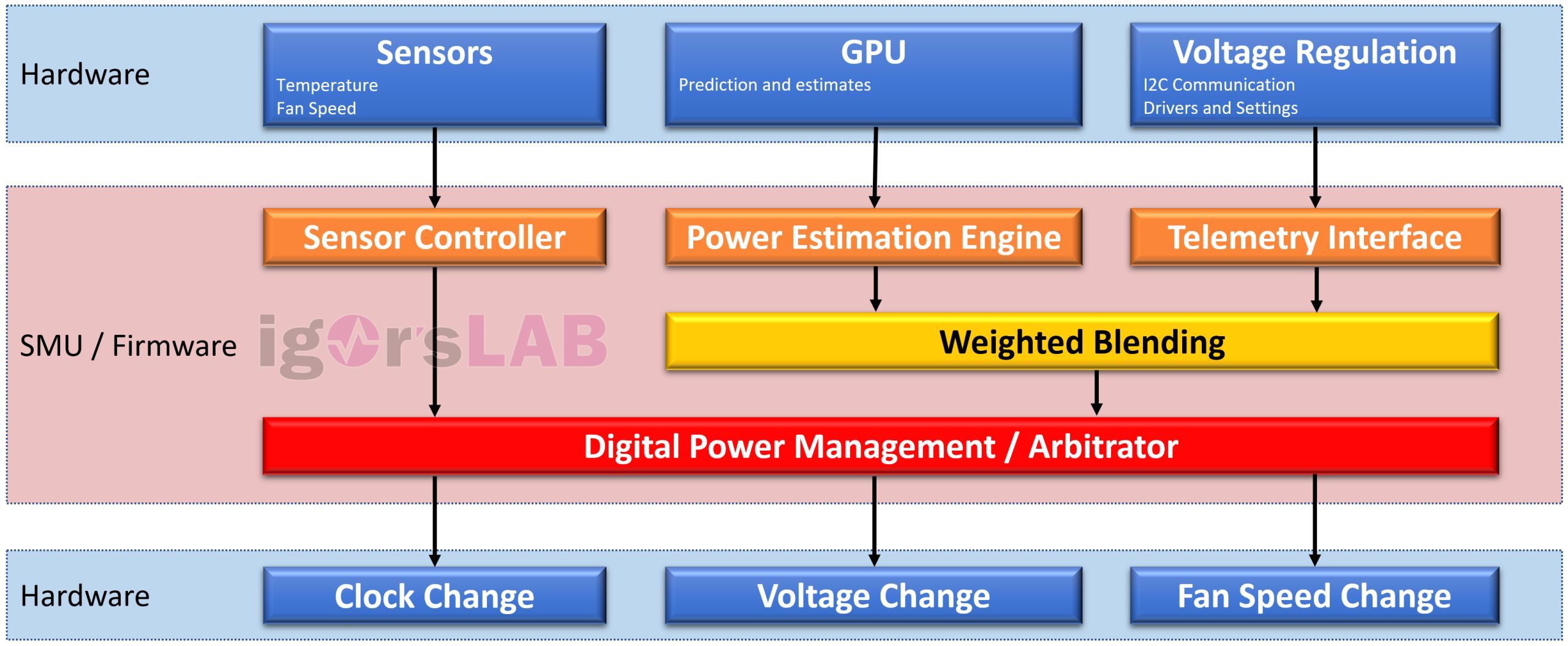
For now, let’s just call it a voltage curve (I’m sure everyone has heard this before), although I’ll have to go into more detail later. To put it in ready-to-use terms: The single boost steps including the default voltage were stored, whereby the clock of the lowest boost step is shifted or fixed by a so-called offset and the rest then results from the calculations of the arbitrator (mediator). With AMD, one sets the clock rates and voltages for some given DPM states, which is much less accurate (more granular), but works similarly in the end.
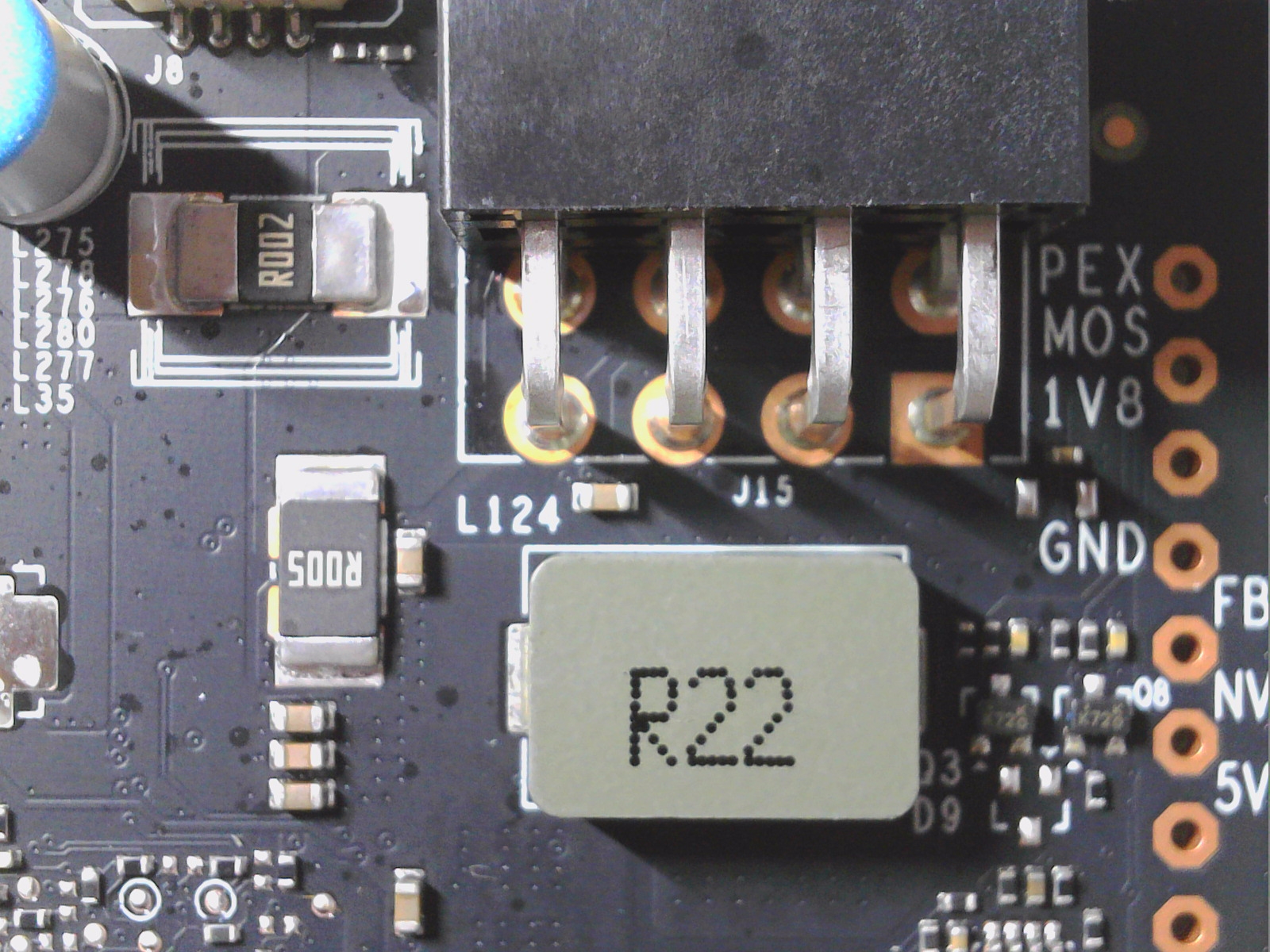
The firmware constantly estimates the energy consumption in very short intervals (quasi in real time), simultaneously queries all the sensors as well as the GPU prediction and includes the telemetry data of the voltage regulator or the input monitoring (shunts, picture below). These values are sent to the pre-programmed DPM (digital power management), i.e. the arbitrator (mediator). This control complex also knows the power, thermal and current limits of the GPU (BIOS, driver), which it can read from the respective registers. Within these limits, it now controls the temperatures, all voltages, clock frequencies as well as the fan speeds and always tries to get the maximum performance out of the card. If even one of the input values is exceeded, the mediator can reduce the voltage or clock.
The disadvantage of such a publicly visible (and with suitable software also customizable) “frequency/voltage curve” is that you can’t actually set it so easily across the board. What the end user can actually only modify is a certain partial shift on the basis of previously calculated, individual limit and reference values of each individual chip under the current conditions! This is where the so-called VFE ( Voltage Frequency Engine) comes into play, providing a flexible framework to specify or evaluate the relationship between clock frequencies, which is normally a function of voltage, speedo and temperature. Or to put it briefly in a nutshell: The determined voltage for each of these frequency points of such a curve is actually a function of the GPU’s speedo, which is determined by “Continuous Virtual Binning”.
You guessed it, now it gets a bit trickier. We like to remember the first paragraphs about binning and the ATE flow: Continuous Virtual Binning (CVB) uses statistical models and algorithms to continuously and virtually analyze the performance of semiconductor devices instead of actually testing them physically. “Continuous Virtual Binning” in our GPU case thus means that the voltage decreases (based on a linear or quadratic equation) by 10 mV (regular step size) when the speedo is increased by the same amount. The voltage for each frequency point is a function of the GPU’s temperature.
The clock frequency and therefore the voltages of the GPU depend on the temperature. Semiconductors (p-type and n-type) can have either a positive or negative temperature coefficient and as the temperature increases, the motion in MOS transistors can decrease. This decrease increases the threshold voltage (Vt). This makes the transistor slower. Therefore, an increase in temperature will decrease the clock frequency and vice versa. This temperature dependence is captured in the same quadratic equation that uses the chip’s Speedo. Since the frequency specified in the steps must logically remain locked, the voltage increases as the temperature increases to still reach the requested frequency (or vice versa). This quadratic equation, which captures the relationship between frequencies and their corresponding voltages, is captured by the so-called VFE frame, which is stored on the chip’s EEPROM as part of the configuration data in the VBIOS firmware and cannot be overwritten.
The main function of the VFE is thus to dynamically adjust the voltage and frequency of the processors to optimize performance and energy efficiency. The VFE works closely with the PMU (Power Management Unit) to provide the correct voltage and frequency values for various operating conditions and load conditions. I’ll get to that in the next paragraph. In summary, the Voltage Frequency Engine and Speedo work together to optimize performance and energy efficiency. The VFE is responsible for adjusting voltage and frequency, while Speedo monitors PVT variations and provides the necessary information for the VFE to make the proper adjustments.
So, now we better take a breath first. Whereas it’s not as complicated as it might read the first time. To make a long story short: You can’t trick or override the Speedo. What can be changed manually is always based on the stored Speedo and the values of the VFE, on which the end customer also has no influence. And now we also know that good cooling is often worth more than the most brutal OC. It’s the dreaded dog-tail principle with air-cooled cards, where increasing the power limit for a higher clock also leads to higher temperatures and thus lower clock rates again. You can do this forever and the card won’t get faster. Only thirstier. That’s exactly why the opposite undervolting is so clever, because it enables higher boost steps due to lower temperatures. So quasi lossless OC for free.

And how is all this initialized and queried at runtime?
The so-called PMU init phase (Power Management Unit Initialization Phase) is the focus here. This is a step in the startup process of systems based on a Power Management Unit (PMU), which provides the various voltage and power supply levels. During this phase, the basic functions of the PMU are initialized, i.e. initialization of the voltage regulators, setting of power supply thresholds, configuration of power-on-reset (POR) and initialization of power-good signals.
As with all configuration data, the NVGPU driver first reads this configuration data from the VBIOS firmware and passes it to the PMU microcode perf task during the GPU initialization phase. During the PMU init phase described above, the perf task also reads the GPU’s Speedo and caches it. It then samples the GPU temperature and solves the VFE equation for each frequency point in the V/F curve.
In the PMU runtime phase (see schematic at the top of the page), the perf task then takes samples of the GPU temperature, among other things, every 200 ms (programmable), for example. If the temperature exceeds a (programmable) hysteresis value, the V/F curve is re-evaluated by solving the corresponding VFE equation and reprogramming the AVFS hardware. And this nice loop is repeated by the card until we dutifully turn off the computer again.
Summary and conclusion
Especially this second page shows that the “curves” that can be changed in the GUI of some programs have an unchangeable basis and that we as end users are only allowed to push some offsets back and forth in the end. The genes are identical for all cards with the same chip, only the performance or the energy required for it will differ. What can then be changed manually only plumbs the upper and lower limits of the respective “bucket” from which the chip originates. Because there are still significant differences.
And to come back to the GeForce RTX 4070: everything can, but nothing has to! Therefore, you should be rather cautiously optimistic about the 215 watt cards. At the moment, everything still seems to work well, but NVIDIA certainly wouldn’t be NVIDIA if there were such gifts all year round.

Danke für die Spende

Du fandest, der Beitrag war interessant und möchtest uns unterstützen? Klasse!
Hier erfährst Du, wie: Hier spenden.
Hier kannst Du per PayPal spenden.
You may also like


About the author
Igor Wallossek
Editor-in-chief and name-giver of igor'sLAB as the content successor of Tom's Hardware Germany, whose license was returned in June 2019 in order to better meet the qualitative demands of web content and challenges of new media such as YouTube with its own channel.
Computer nerd since 1983, audio freak since 1979 and pretty much open to anything with a plug or battery for over 50 years.


49 Antworten
Kommentar
Lade neue Kommentare
Mitglied
Urgestein
1
Urgestein
1
Mitglied
Urgestein
1
Mitglied
1
Mitglied
1
Urgestein
1
Veteran
Urgestein
1
Urgestein
Urgestein
Alle Kommentare lesen unter igor´sLAB Community →