


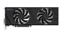
Board layout
Sapphire differs significantly from AMD's reference design when designing the board. This even makes sense in many places, as the cooling has been optimized and is in the foreground. By eliminating the external memory modules, as on the reference board, the power supply can be distributed around the package somewhat more worry-free. We see a neat 7+1 phase design for GPU and memory, as well as other voltage converters for the respective partial voltages. We will, of course, deal with all these things in more detail in a while.
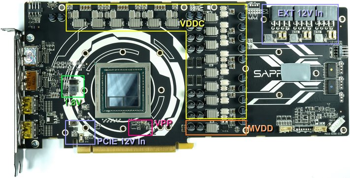
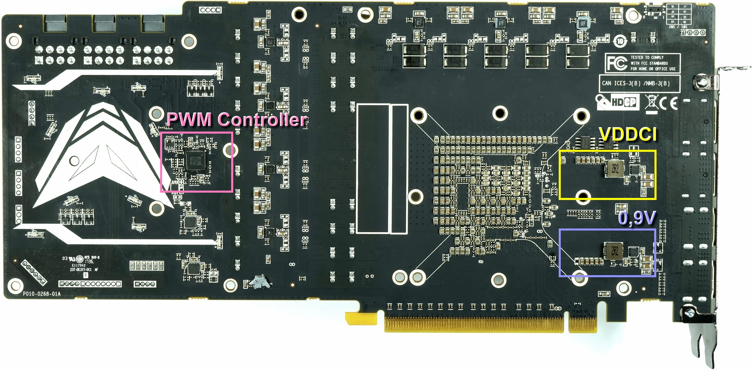
The three 8-pin connectors are each connected over a coil, which helps to smooth certain voltage peaks. However, we could not find larger capacitors here. On the back, besides the very tightly equipped base of the package, we see the PWM controller as the most obvious part, as well as other components, which we will discuss further. With the MLCC below the package, X6S is also sufficient, because the temperatures should remain low enough thanks to the excellent cooler and therefore you do not have to resort to 125°C-class products for safety reasons.
Power supply connections
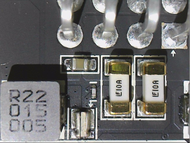
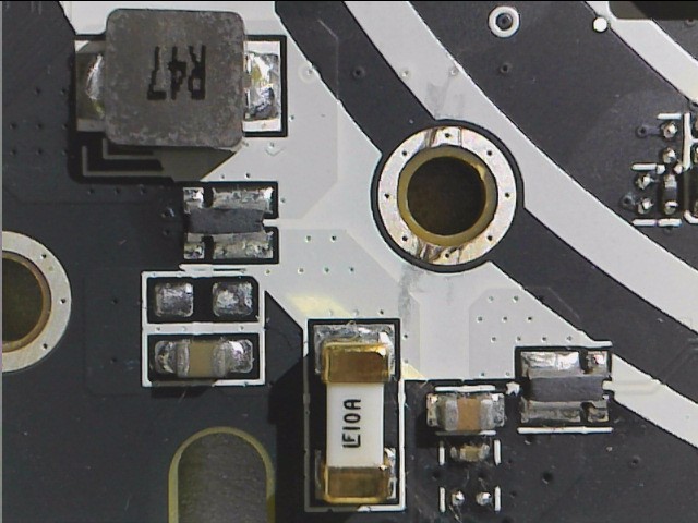
Sapphire relies on a total of three external sockets, each of which is secured by two 10A fuses connected in parallel. Each of these connectors uses a coil as a filter in the input area, which is quite laudable to slightly reduce the interactions between the graphics card and the power supply (peaks). The power supply via the motherboard also relies on a (single) 10A fuse, as well as on a normal coil with encapsulated ferrite core.
 |
 |
Those who now miss the usual shunts can be reassured. Since Vega does not support input monitoring, these shunts can be omitted. Instead, one relies exclusively on the control of the outgoing flowing currents, which is quite easy to realize with digital PMW solutions.
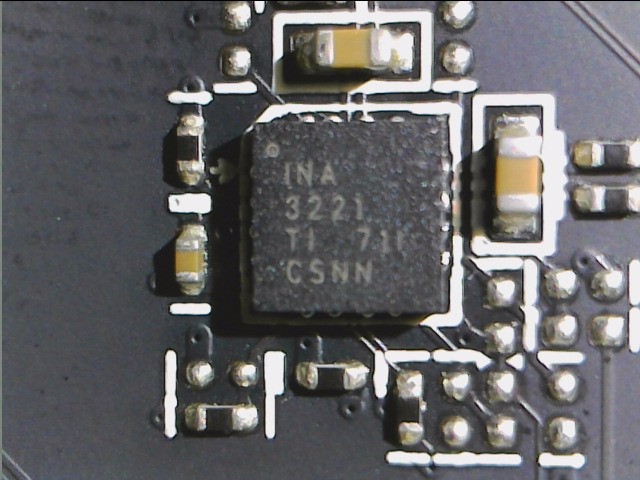
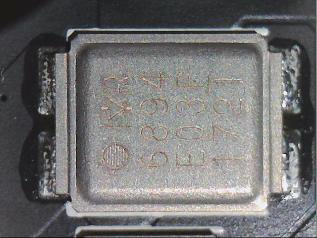
For voltage control, we find two InA3221 from Texas Instruments on the back of the board, which are triple-channel monitoring chips for the high-side and bus voltages, which also support the I2C and SMBUS interfaces.
GPU Power Supply (VDDC)
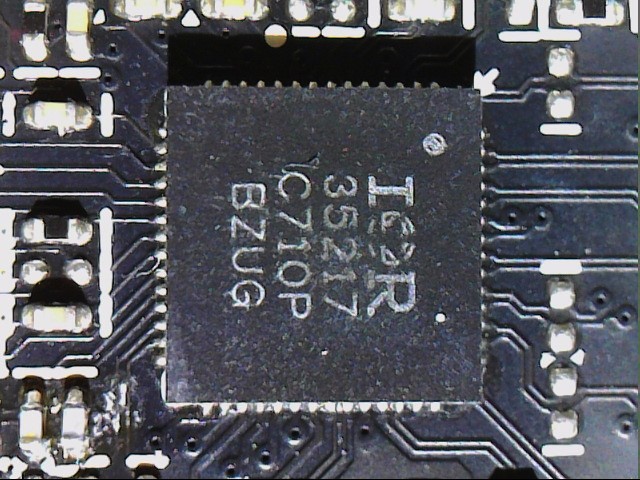
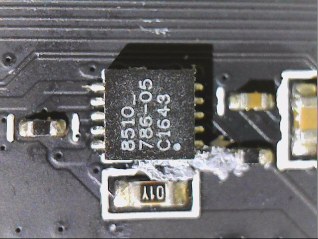
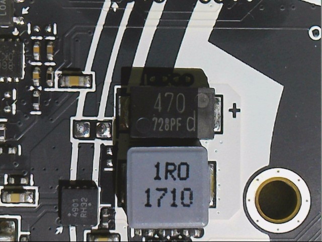
As with the reference design, the focus is first on the IR3521 from International Rectifier on the back of the board, a dual output digital multi-phase controller that can provide both the 7 phases for the GPU and a further phase to which we will still be discussed. But back to the GPU and thus to what we see in the schema above as a VDDC block. We count 14 voltage transformer circuits, not seven. However, since only seven real phases are created, you double each of these phases in order to be able to divide the load into two converter circles per phase.
 |
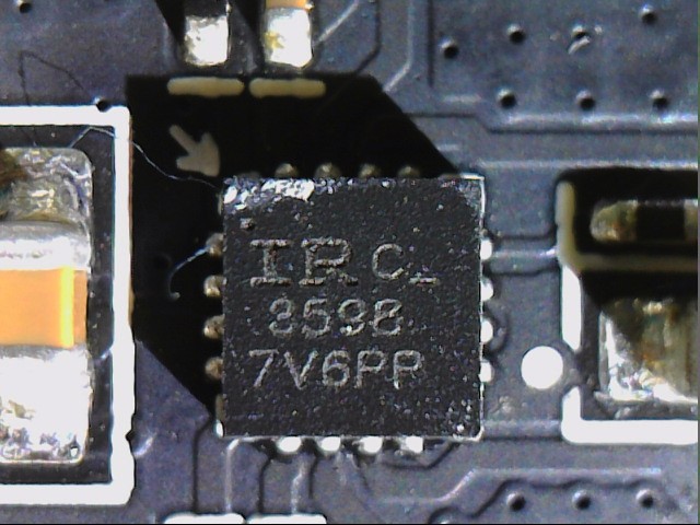 |
A total of seven IR3598s are used for this so-called doubling, which are located on the back of the board. The actual voltage conversion of each of the 14 converter circuits is each performed by an IRF6811 on the high side, as well as an IRF6894 on the low-side, which also contains the required Schottky diode. Both are heXFETs from International Rectifier that have been used by AMD before.
 |
 |
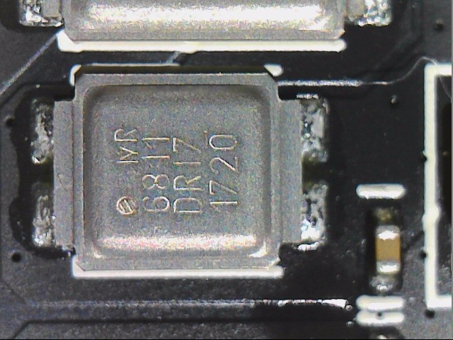
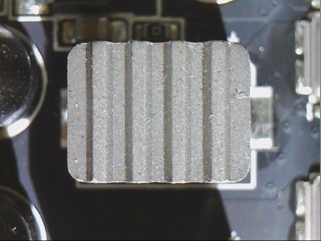
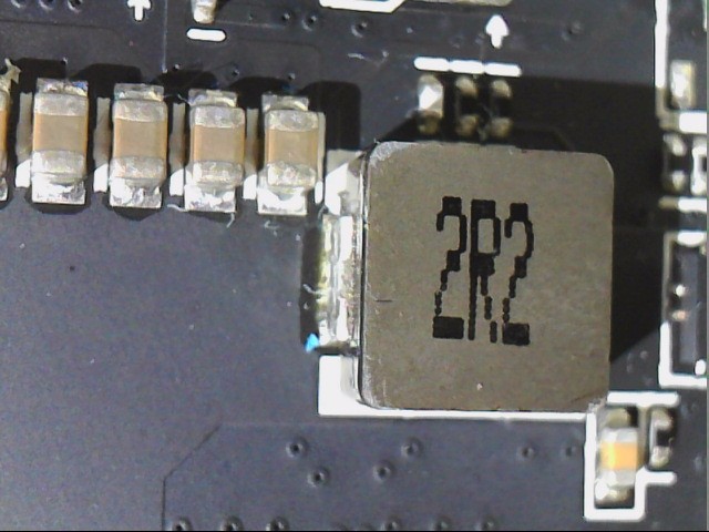
For the coils, AMD relies on what is often referred to as black diamond choke for both the VDDC and MVDD areas, which are in effect specially encapsulated ferrite core coils, but which additionally provide a kind of cooling fins on the surface. Were. For the other coils, such as the partial voltage ranges or in the input filtering, the usual encapsulated ferrite core coils are then used again without additional frills.
 |
 |
Power supply of the memory (MVDD)
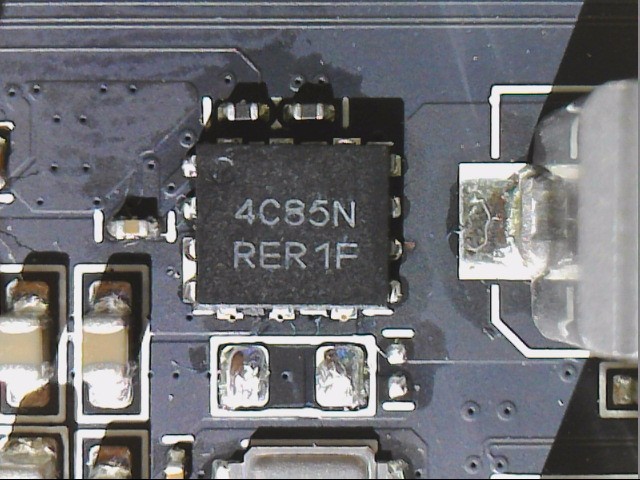
As mentioned briefly, the IR35217 also provides one phase for storage. One phase is sufficient for the card, as the memory is much more sufficient. The gate-driver CHL815 is back on the back of the board, while an NTMFD 4C85M from ON Semiconductor is used for voltage conversion. This dual N-Channel MOSFET realizes both the high and the low-side.
 |
 |
Other voltage converters
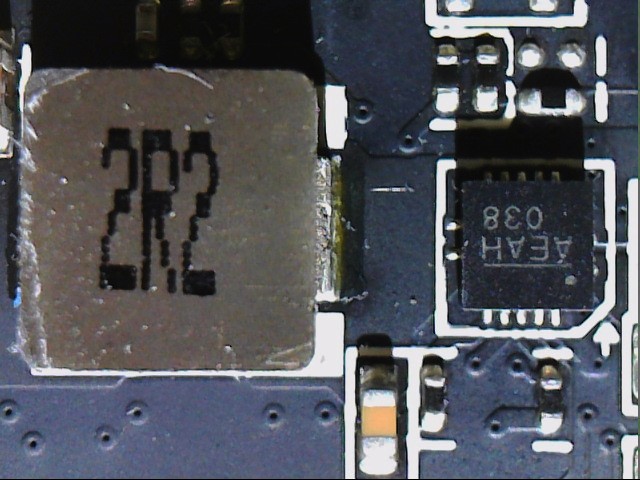
The production of VDDCI is not a big item in terms of performance, but it is important. It is used for GPU-internal level transition between the GPU and memory signals, something like the voltage between the memory and the GPU core on the I/O bus. In addition, a constant source for 0.9 volts is generated. These two very similar voltage converters are located on the back of the board.
 |
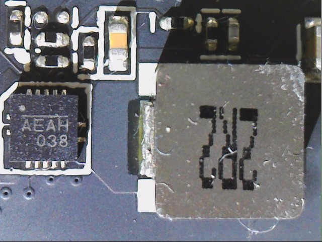 |
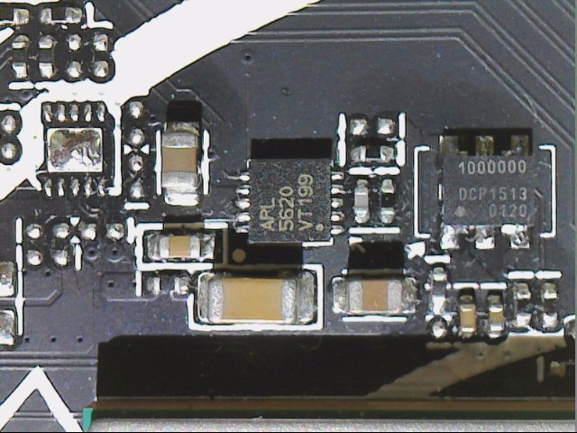
Below the GPU you can also find the APL5620 from Anpec for the VPP on the top of the board. This ultra-low dropout chip generates the very low voltage for the Phase Locked Loop (PLL) range. There is also a 1.8V source (TTL, GPU GPIO) on the front side.
 |
 |
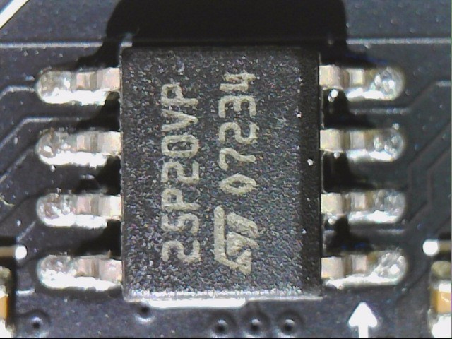
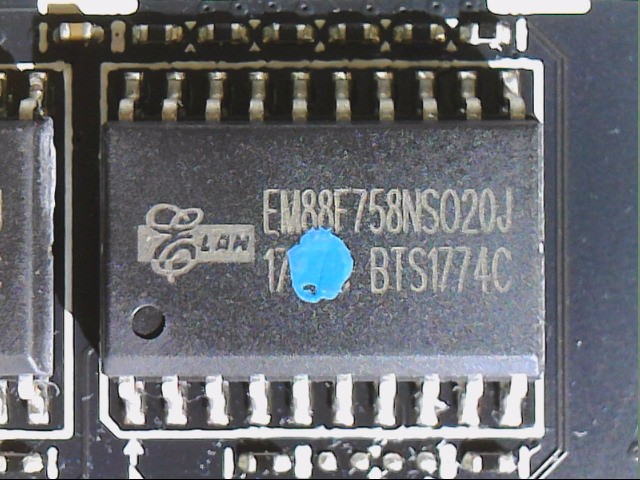
So we would almost be through, because the rest is the usual standard. Only the two separate BIOS chips ST25P20VT from ST Microelectronics, as well as two programmable 8-bit controllers EM88F758N from Elan, with which, among other things, are still striking. RGB effects and fan control can also be realized.
 |
 |
- 1 - Einführung und Kartendetails
- 2 - Spannungsversorgung und detaillierte Platinenanalyse
- 3 - Ashes of the Singularity: Escalation (DX12)
- 4 - Battlefield 1 (DX12)
- 5 - Destiny 2
- 6 - Tom Clancy’s The Division (DirectX 12)
- 7 - Doom (Vulkan)
- 8 - Tom Clancy’s Ghost Recon Wildlands (DX11)
- 9 - Metro: Last Light Redux (DX11)
- 10 - Middle-earth: Shadow of War (DX11)
- 11 - The Witcher 3 (DX11)
- 12 - Leistungsaufnahme im Detail
- 13 - Temperaturen, Taktraten, OC und Wärmebildanalyse
- 14 - Kühlerdetails und Geräuschentwicklung
- 15 - Zusammenfassung und Fazit


Kommentieren