


Foreword to the Radeon Tweaker Group project
No, we are not hosting the original RTG (Radeon Technology Group), but a group of those who have made it their mission since AMD's Polaris and later Vega to make some over-voltage and unnecessarily hot Radeon what you would like as an end customer to do. : to a faster and much more efficient graphics card.
The unofficial RTG (Radeon Tweaker Group) offers the technical solutions and ideas with the help of various conversion and cooler mods up to the popular files for the PowerPlayTable.
![]()
And in order not to decorate myself with foreign feathers, the thanks for the work done over the years go especially to Gurdi, Hellm, Vento and the R.B.R.T. (Red BIOS Rebellion Team). For the time being, I only deliver the virtual home, a logo and some support, but I will soon be involved in the content with my laboratory and the measuring possibilities. Because in the end you have to be able to prove exactly what you have worked out. And yes, it's really worth the effort.
Maybe we will soon also get a first water block for the map, then of course there are also the tests here on the page. Promised! You can stand on the map as you like, but it is and remains a thankful field for your own improvements or improvements. Modifications.
For the time being, however, we will host everything about the current Radeon VII here on igor'sLAB, but I am sure that we can also integrate the "older" maps in a timely manner. Then you as a visitor get everything from the above-mentioned team from a single source, including competent forum support and the usual YouTube cancellation with the right news for the smartphone generation. You will find here on the right our normal article navigation and I will update this article continuously and also create a fixed link.
-
Subvolten: Increase in efficiency and sweet spot with detailed measurements
-
Cooler modifications ("Ghettomod" etc.) and Raijintek Morpheus
-
Explanation and assistance for the PowerPlay tables (PPT)
-
Overclocking with the PPT to the maximum
-
Water cooling (in progress)
The most important things about the power supply of the Radeon VII
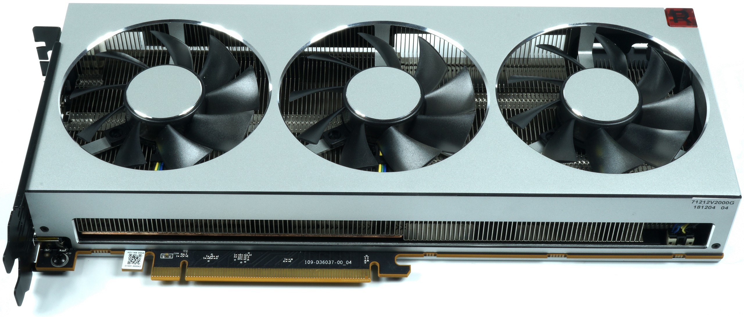
If you don't know my launch article about the Radeon VII, I've summarized the details again, because what AMD has put on the board here is actually technology at its finest. It is even worth to watch the video below with the detailed analysis (if you haven't already done so) to get in the mood for the following video. At first glance, the entire layout looks clear and well thought out, and the manufacturer relies on very low components and components, also due to the 2-slot design, in order to obtain as much volume as possible for the cooler. That, in turn, is very much in our interest.
The external power supply is provided by two 8-pin connectors, which sit at the top of the board, as is common for consumer cards. You could have turned the sockets 180° to save even more space, but it actually fits that way. The topology of the power supply has turned out a little more complex this time and simply counting so coils does not help you to learn the whole truth. Because AMD generates a lot of partial voltages, which you have to assign correctly first.
For the generation of VDDCR_GFX (in the picture below red), i.e. the voltage of the GPU, 5 output phases are generated with the help of an IR35217 (located on the back of the board) of International Rectifier. With the help of one IR3599 (also International Rectifier) per phase, a phase multiplier chip ("doubler"), two voltage transformer circuits are then connected to each of these 5 phases, which work slightly phase-shifted. In this way, you get 10 voltage converters at the end.
To do this, you will then rely on 10 Power Stages TDA21472 from Infineon, i.e. highly integrated solutions that combine a complete voltage converter including high- and low-side, the gate-driver and the Schottky diode, as well as a control MOSFET in a common package. . As with Nvidia's solution, the TDA21472 relies on a true MOSFET DCR and no longer on the much more inaccurate (and cheaper) Inductor DCR. These values for current flow and temperatures are then used by the arbitrator for a smarter control of the processes.
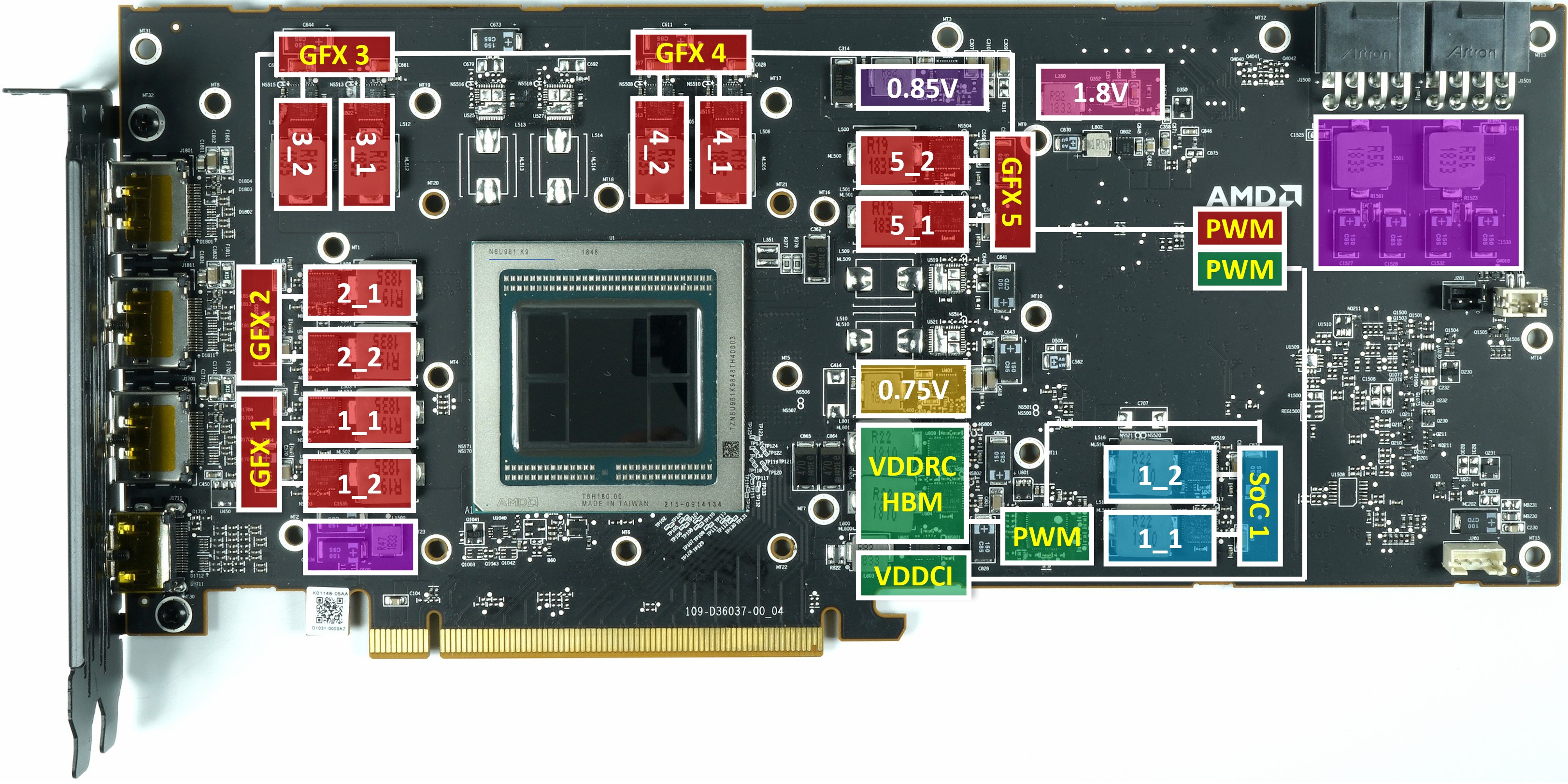
However, because the IR35217 is a true multi-phase controller that can provide up to 6+ 2 phases, the second part of the controller is used for the independent deployment of the VDDCI_Mem. The explanation of what VDDCI_Mem is in the video. As a voltage converter, you rely on an IR35401M, which is a slightly simpler PowIRstage. With the memory, however, it becomes very tricky now. On the front of the board you will find another PWM controller of type IR35217. On the one hand, this generates the two real (and not double) phases for VDDCR_HBM, i.e. the power supply of the four HMB2 modules on the package.
Here, too, two TDA21472s are used, each of which is addressed directly by the controller. The controller also provides the VDDCI_SoC (blue). Here, however, only one phase is generated, which then splits by means of an IR3599 on two phase-shifted voltage converters with each TDA21472. The remaining partial voltages of 1.8V, 0.85V and 0.75V are generated separately by simpler Buck controllers. It is interesting that AMD completes all 12V rails with neat LC-members, which should smooth the spikes properly, since in addition to the usual longitudinal coils, the appropriate capacitors are also used. So that all fits.
The bottom line is that this layout, including assembly, is also suitable for proper overclocking tests, provided that the cooling is correct and improved. And if you don't want to switch to water, because there are no water blocks (yet) or because you prefer air: we also offer mods with the original cooler, which already deliver a decent added value. But more in an extra chapter!
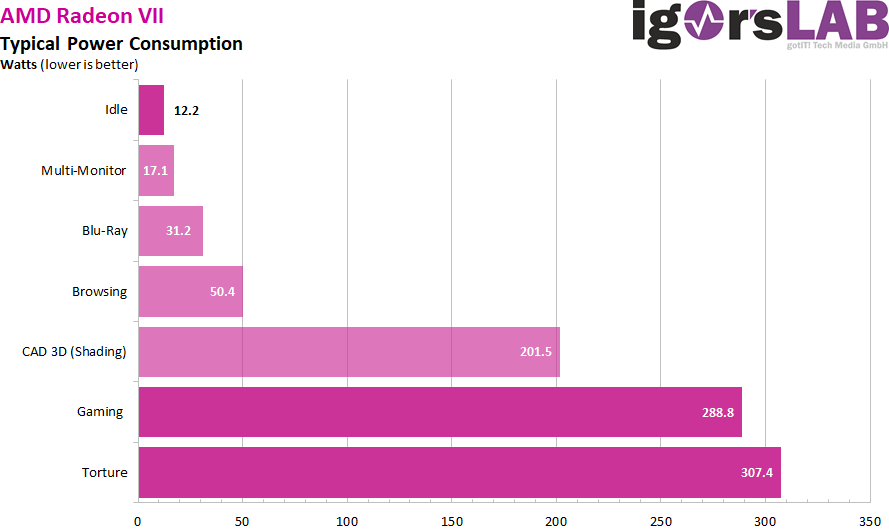
Power consumption and temperatures of the original card
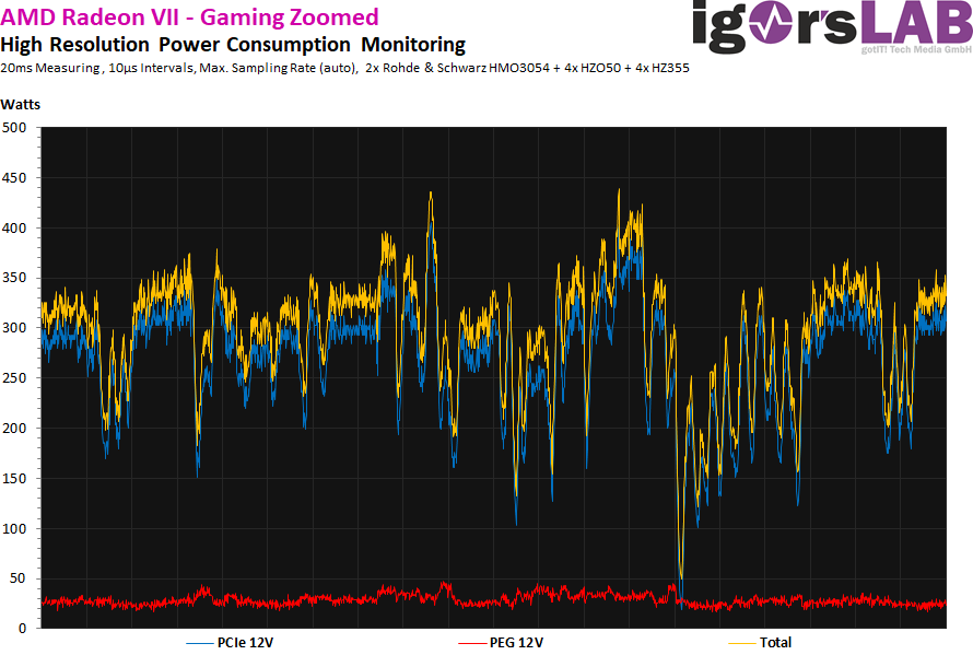
Measurements were made in the laboratory under conditions as realistic as possible. The power consumption of this card is approx. 12 watts in the idle very good in the race. With the gaming loop, you are in the range of the propagated TBP of 300 watts with just under 289 watts and in the Torture loop with a good 307 watts. You get the card in 4K or 5K resolutions also with the gaming loop just over 300 watts, if you provoke it and e.g. fully utilized the memory.
As I have already demonstrated in detail in my basic article "The fight of graphics card against power supply – power consumption and load peaks demystified", there are also temporarily higher loads in the millisecond range, which are unfavorable in case of unfavorable designed or improperly equipped power supplies can already lead to unexplained shutdowns. The TBP (Typical Board Power) measured by the graphics card manufacturer or the reviewers does not really help for a stable design of the system.
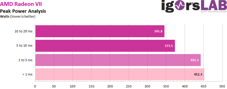
Peaks with intervals between 1 and 10 ms can lead to shutdowns with very fast-reacting protective circuits (OPP, OCP), especially for multi-rail power supplies, although the average power consumption is still in the norm. For this card/ I would therefore calculate at least 370 to 400 watts for the graphics card firmly, if you don't want to experience any nasty surprises. If you rely on Noname power supplies, you should use the 400 to 450 watts as a guide, you never know…


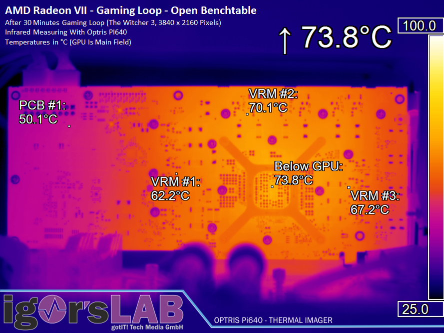
The temperatures of the original card were approx. 73 to 74 °C in Witcher 3 and Ultra-HD at maximum settings, which roughly corresponds to the board temperature below the Interposer package. The clock was average after 30 minutes of continuous load at 1732 MHz. Only the fan speeds of a whopping 2935 rpm are completely unacceptable because they are too noisy.
- 1 - Vorwort zur RTG
- 2 - Untervolten mit dem Wattman leicht gemacht
- 3 - Leistungsaufnahme und Temperaturen mit Low Voltage Settings
- 4 - Lüfter-Umbau mit Originalkühler (Ghetto-Mod) und dem Raijintek Morpheus
- 5 - Erklärung und Hilfestellung zu den PowerPlay-Tabellen (PPT)
- 6 - Übertakten mit den PowerPlay Tabellen und Fazit


Kommentieren