


Board analysis and power supply
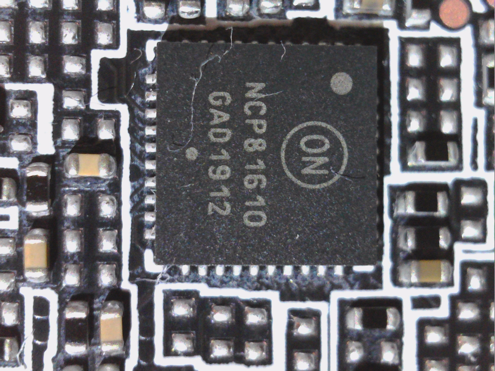
The board is also based on the well-known PG132 reference design, a 12-layer board with backdrill method. If we now take a look at the upper side of the board, we can see the division of the main power supply. NVVDD stands for the conventional core voltage, which is what we like to call GPU voltage. Here there are a total of eight individual phases (one less than with the FE), which are provided by an NCP81611 from ON Semiconductor on the back. This is a digital PWM controller with VID interface, compatible with NVIDIA’s Open VReg specification. The NCP81611 can generate up to 8 phases, so it is sufficient. These eight phases are each equipped with slightly cheaper 50-A powerstages AOZ5311NQI from Alpha & Omega, which do not provide true MOSFET DCR, but do offer a temperature protection circuit and readout output.
The assembly of the second GPU power supply MSVDD, which I had called “Gedönsspannung” and which stands for “Miscellaneous”, is very similar. We find a total of five individually controlled phases generated by an NCP81611 from ON Semi. The five power days are the same as for NVVDD. So in the end there are 13 phases for the GPU alone and the different voltages for the GPU. This should also make power gating in the GPU a bit easier, although AMD uses a similar, if much smaller, outsourcing with VDDCI. The voltage range of both ranges is between 0.7 and a maximum of 1.2 Volt, whereby the maximum value can never be reached by the end user without special firmware and software. However, the minimum value is important, so there are technical limits for undervolting, but NVIDIA assigns them to everyone.
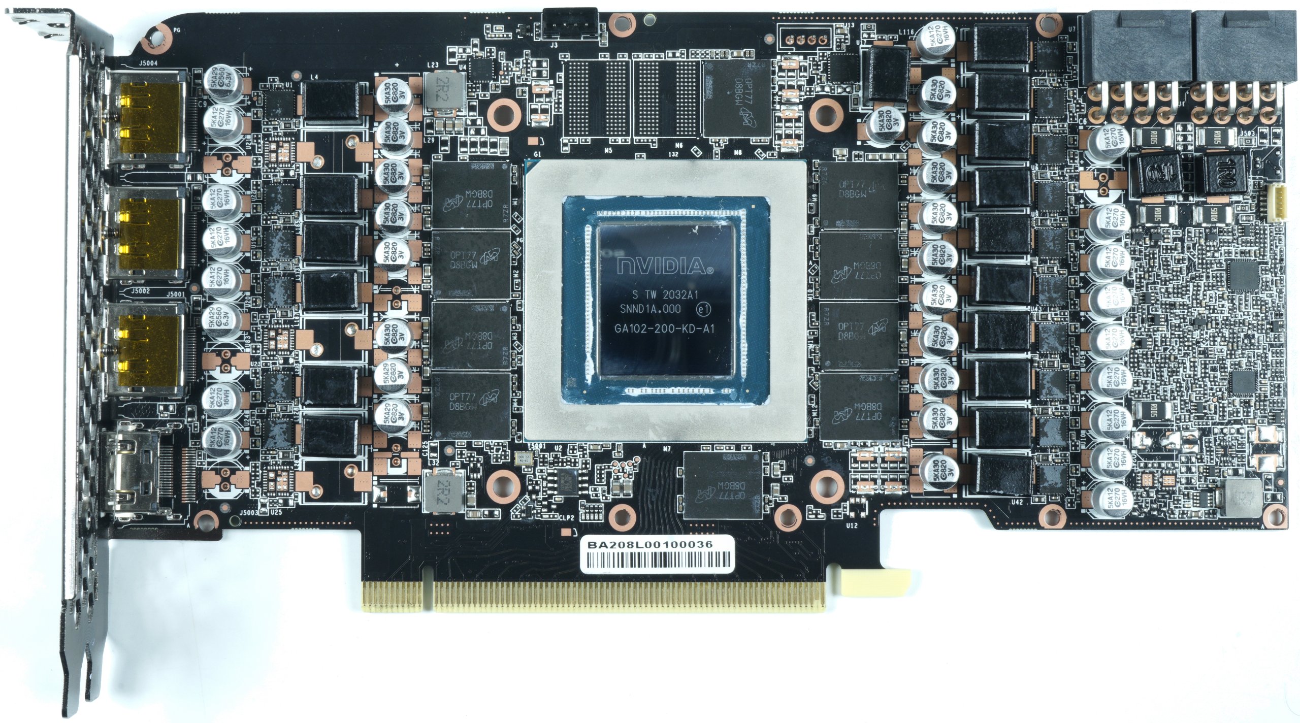
For the memory NVIDIA uses three phases, which also rely on the well-known power stages of Alpha & Omega. The PWM controller in the form of the NCP81611 is located on the rear side, as is the one for MSVDD. The power stages of the PCI Express voltage PEXVDD and the 1.8 Volt are located on the front side together with the corresponding coils. The capacitor six-pack on the bottom of the BGA contains a MLCC combination and 5 SP-CAPs, is sufficient.
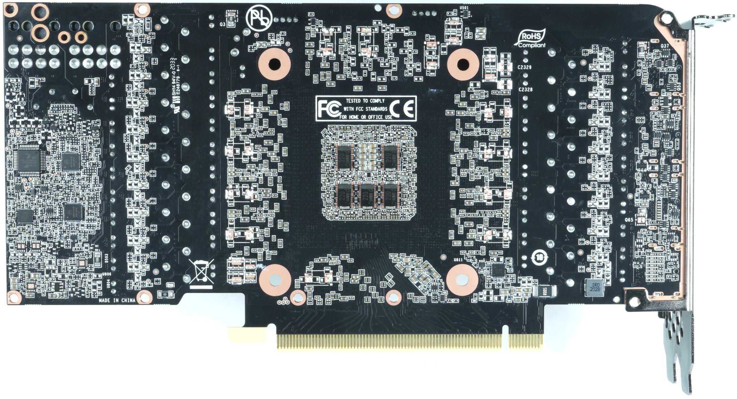
For input smoothing, three coils with 1 µF each are used, behind which a shunt is located, over whose voltage drop the flowing currents are measured. On the right side we see the PWM controller NCP81611 from ON Semiconductor, which is used for NVVDD.
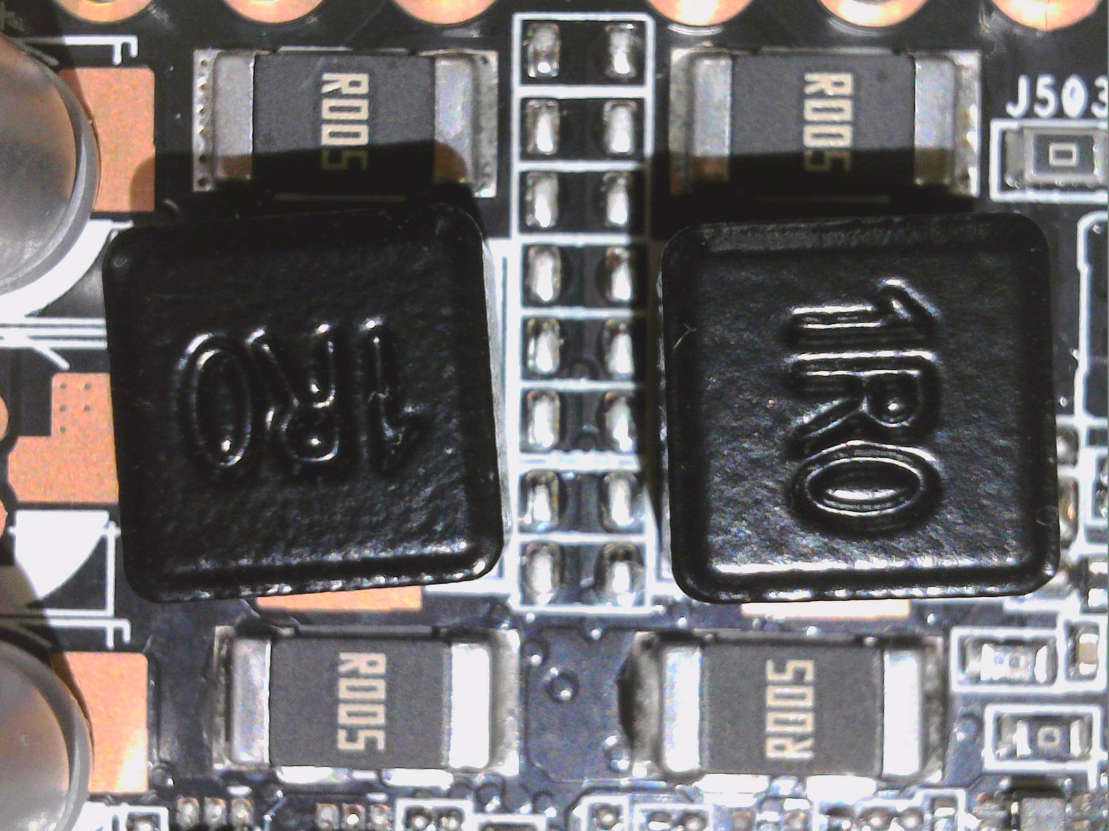

The following two pictures show one of the power stages of type AAOZ5311NQI from Alpha & Omega, which is used in all three major power supply circuits, and one of the many 220 mH coils. On the right side we see one of the two NCP81610 for MSVDD and the memory.

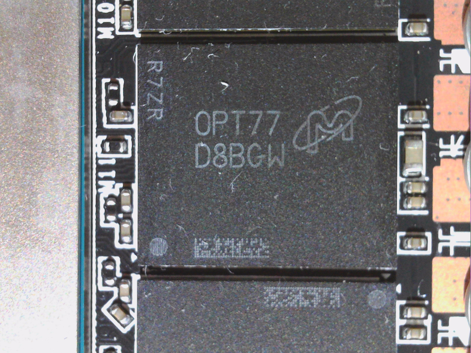
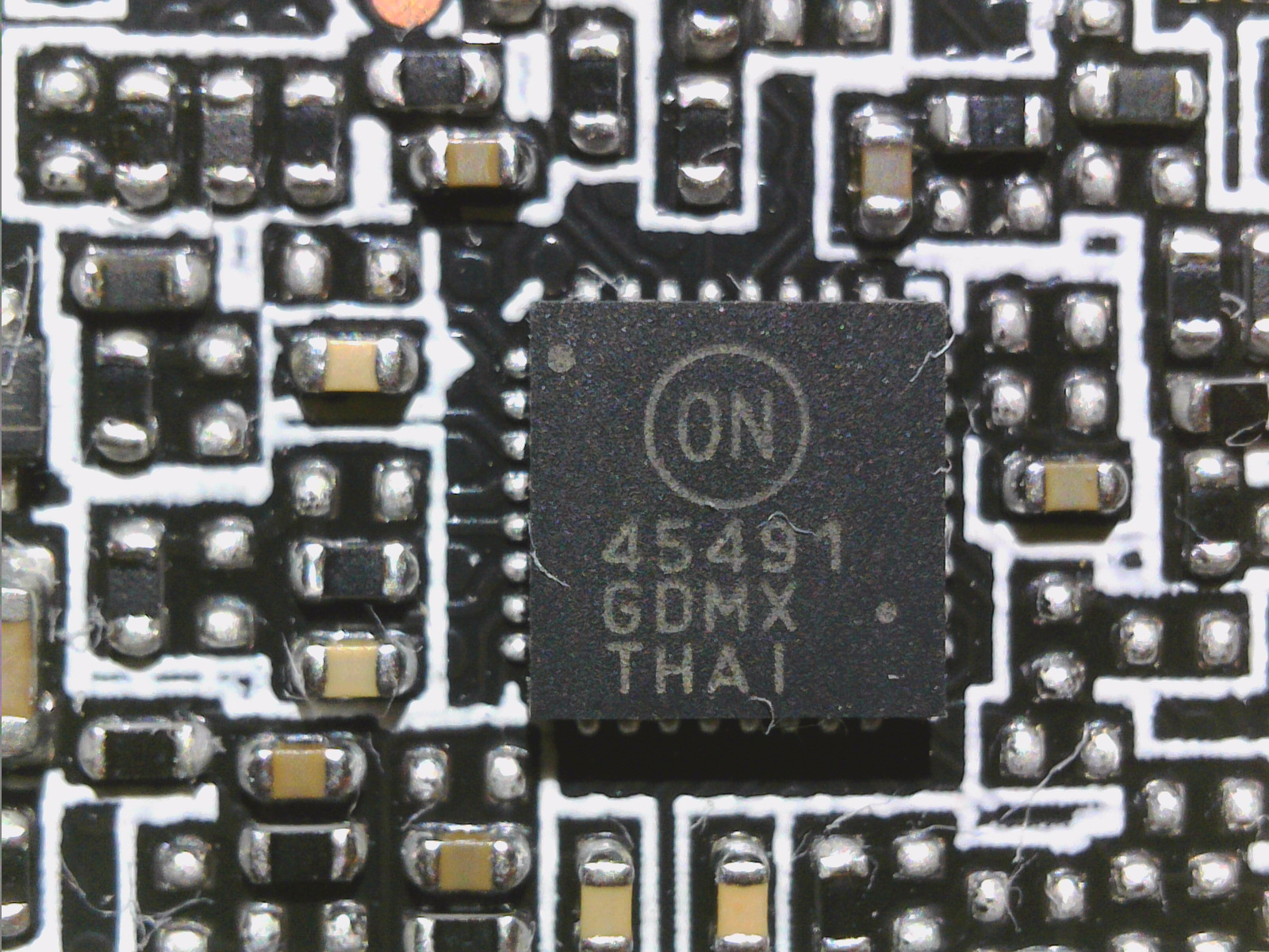
We see below one of the memory modules from Micron. The total of ten 1 GB modules of the GDDR6X memory come from Micron. The memory runs at only 19 Gb/s, although it could actually run at 21 Gb/s. The extent to which NVIDIA wanted to prevent thermal problems here can of course only be speculated. On the right side of the picture the monitoring chip NCP45491 for voltage and current monitoring of ON Semi.
Cooler and disassembly
Above the heatsink and the partially open structure behind the short board are a total of three PWM-controlled 9.2 cm fans with a rather aggressive rotor blade geometry. But also the maximum speed of the separately controlled fans of up to 4200 rpm is not exactly an expression of noble reserve. Let’s hope that it stays quieter than the card could if it had to or if the user could provoke it with a poorly ventilated case.
The large heatsink cools the GPU, the memory and coils of the large voltage converters and one more MOSFET are cooled by the thermally connected mounting frame. A total of six nickel-plated 6 mm copper composite heatpipes, soldered to the back of the nickel-plated heat sink, ensure the removal of waste heat.
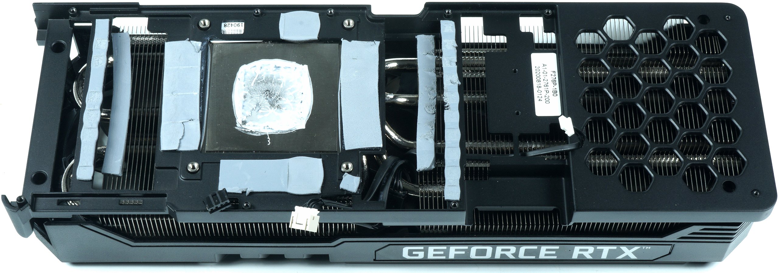
The backplate is also made of light metal with a brownish coating, and the manufacturer thermally bonds the backside under the RAM modules to the backplate, so that it is not only purely optical in nature, but also has a stabilizing effect on the PCB.


Kommentieren