


I wrote it already in the preliminary remark that this time I could and had to rely only on the photos of third parties. The board of the Founders Edition leaves a rather ambivalent impression, because as much as I praised the two reference boards of the GeForce RTX 2080 and 2080 Ti (by the way, rightly so), the shortened board of the GeForce RTX 2070 FE is now much easier . You can see the efforts of possible savings at all corners and edges.
At second glance, something else is missing on the back of the board. Instead of China, as usual, the FE from which these pictures were taken originated in Hong Kong – manufactured by TTM Technologies. I noticed this difference at that time with the GeForce GTX 1060 FE, which, in contrast to the GTX 1070, 1080 and 1080 Ti, was also produced by TTM and not exclusively under Nvidia's own UL number and was also only very sparsely sampled as A FE.

Now you may also need to know that TTM actually stands for "time-to-market" and that this large manufacturer has also specialized exactly in producing time-critical series virtually ad hoc and from the stand. These press samples, which are sent in homeopathic cans and mainly in North America, are obviously not the usual mass production of the in-house cards, but a short-term solution (which has also been quite expensive). should be).
I would also like to apologise for the image quality, as they come from a third colleague who did not really want to test this card and is not equipped with a photo- That's why his smartphone shots have to be enough this time, as annoying as that is in the end for everyone. Let's first take a look at the significantly shortened board with the power supply connection as a kind of flange-buttoned worm progression.
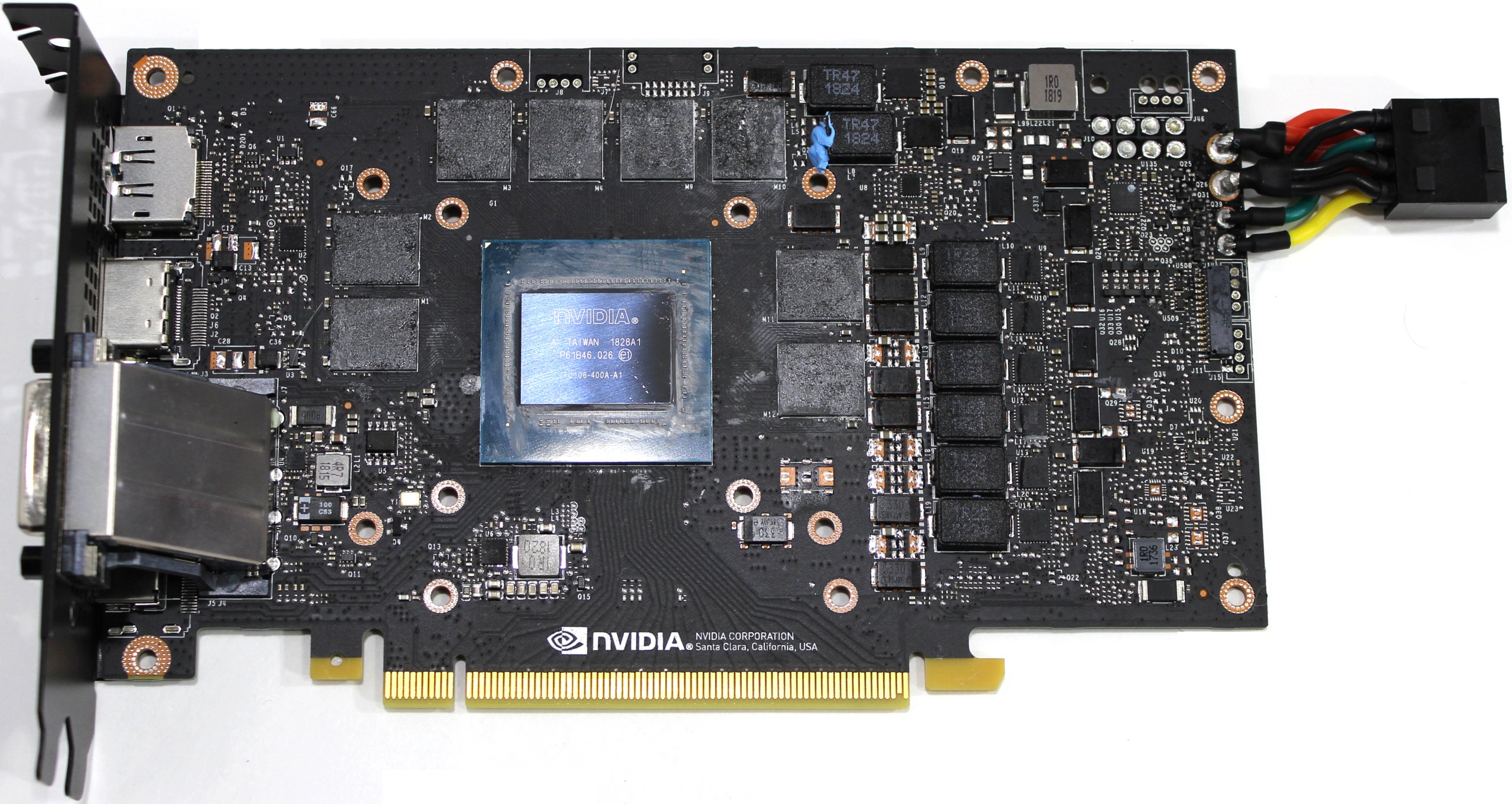
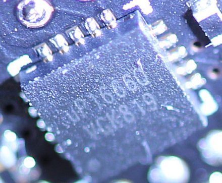
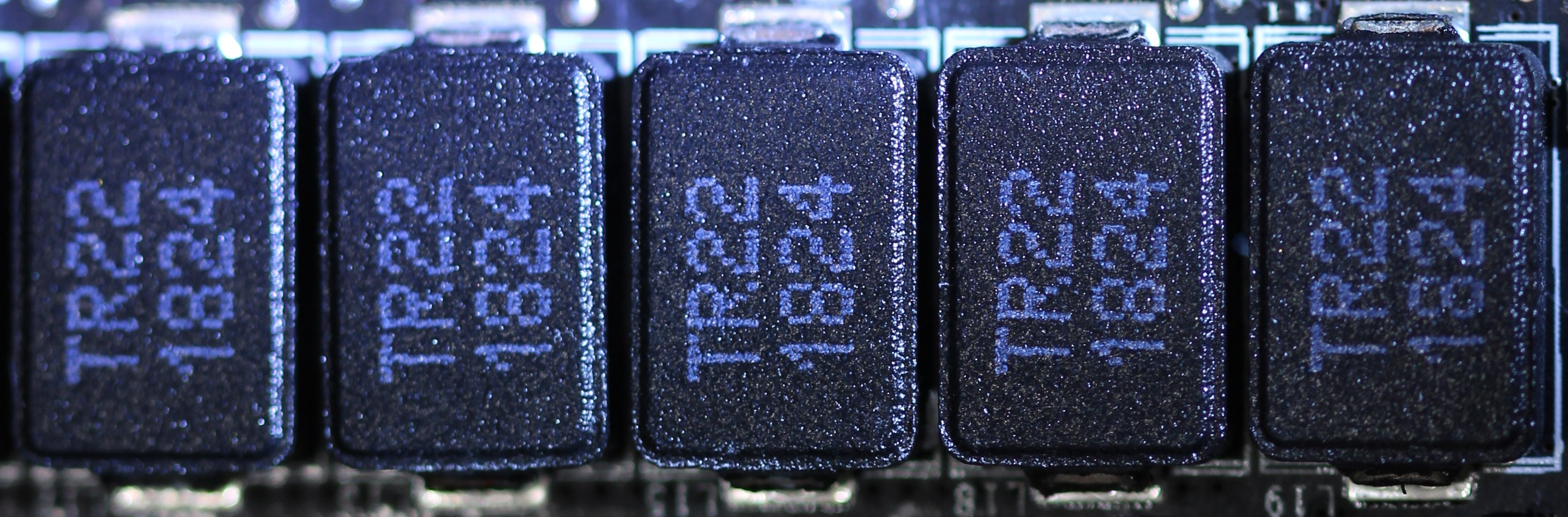
We see six simple voltage converter phases for GPU power supply, as well as two more for memory. For the GPU, you rely on an uP9512R, which could generate up to 8 phases, but only has to deliver 6. The memory is provided by a small uP1666, which only needs to deliver two phases. Both PWM controllers are from UPI.
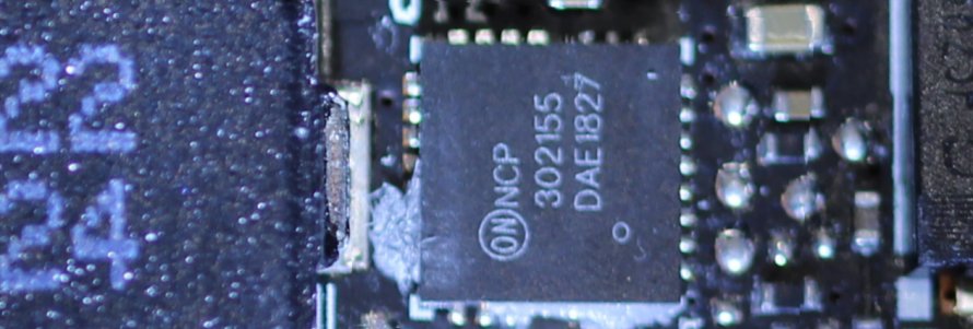
With the NCP 302155 from ON Semiconductor, the nCP 302155 will take over a total of eight (6+2) low-cost dual MOSFETS for the high- and low-side, which also have an integrated driver. The significantly more expensive and better Smart Power Stages of the 2080s cards are dispensed with in favor of costs. However, the monitoring of current flow and temperatures is also eliminated (IMON, TMON).
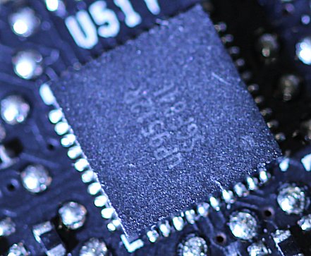
Thus, the GeForce RTX 2070 differs very clearly from what we wrote in the theory article on the 8-phase voltage supply and the quality of the voltages generated. It's a pity, because the PCB really goes more in the direction of GeForce GTX 1060 in complexity. Interesting, however, is the relatively new uP7561Q, a Two Channel Power Input Management IC for monitoring on the back.
The whole thing is smoothed for the GPU with the usual 220mH coils, with the memory it is even some with 470mH. As always, they are encapsulated and encapsulated ferrite core coils, but from a different manufacturer than usual. The fact that the card has a single BIOS is no secret and I couldn't see any other subtleties in the pictures. Which I would be able to get through with.
The label on the memory identifies it as micron's MT61K256M32, as on the GeForce RTX 2080 (T)i. These are 8GB GDDR6 SGRAM modules (2 channels x 256 Meg x 16 I/O, 2 channels x 512 Meg x 8 I/O) with a bandwidth of 14Gb/s. Since a total of eight modules are installed, the memory expansion of 8 GB is also available.
One for all, all on one?
The power supply via an external socket is also, as with the GeForce GTX 1060 FE, rather unusually solved and at least worth questioning in this performance class, especially since the soldering eyes for a native socket are even available this time. But what is it all about? The 6-pin connector of the GeForce GTX 1060 FE had to deliver a total of 62 watts at that time, so that on average approx. 5.2 amperes flowed. Distributed on three veins, which were twisted, tinned and soldered on the printed circuit board in a single soldering eye, this is quite justifiable and also practicable in every respect (see picture).

But such a GeForce RTX 2070 is not a 120-watt graphics card, but Nvidia already gives the power consumption itself and without OC already with 185 watts. This alone is not a broken leg, because the experienced reader actually sees an 8-pin supply connection, which should be easy in theory. With the RTX 2070, however, it looks a bit accustomed to how the cables were combined and soldered. Up to 11 amperes could flow here, whereby the problem should not be the five ground lines (3 + 2), but the three red 12V lines (see picture below).
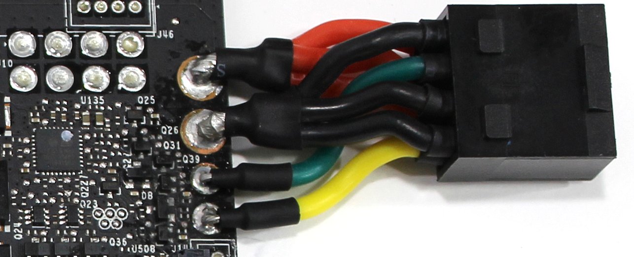
Unfortunately, I can neither confirm nor refute the circulating messages about hotspots at this very point due to lack of IR measurement and thus only pass on what information was available from third parties unvalued. If there is still the possibility of a test of my own later, then of course I will submit this…
- 1 - Vorbemerkung und Einführung
- 2 - Tear Down - Platinenanalyse
- 3 - Ashes of the Singularity
- 4 - Battlefield 1
- 5 - Destiny 2
- 6 - The Division
- 7 - Doom (Vulkan)
- 8 - Far Cry 5
- 9 - Forza Motorsport 7
- 10 - Ghost Recon
- 11 - GTA V
- 12 - Metro Last Light
- 13 - Tomb Raider
- 14 - The Witcher 3
- 15 - World of Warcraft
- 16 - Leistungsaufnahme, Temperaturen, Lautstärke
- 17 - Zusammenfassung und Fazit


Kommentieren