


Teardown: PCB layout and components
Let’s start with the PCB first. NVVDD is the most important voltage and so the result is a voltage converter design with a total of 5 real phases and the resulting 5 control loops for NVVDD alone. So you save another phase compared to the RTX 4070 FE, but this is acceptable considering the much lower TDP. Six phases would have been better for me and certainly more sensible in view of possible hotspots and a higher efficiency. But it should also be about the price and so a compromise has to be made again.
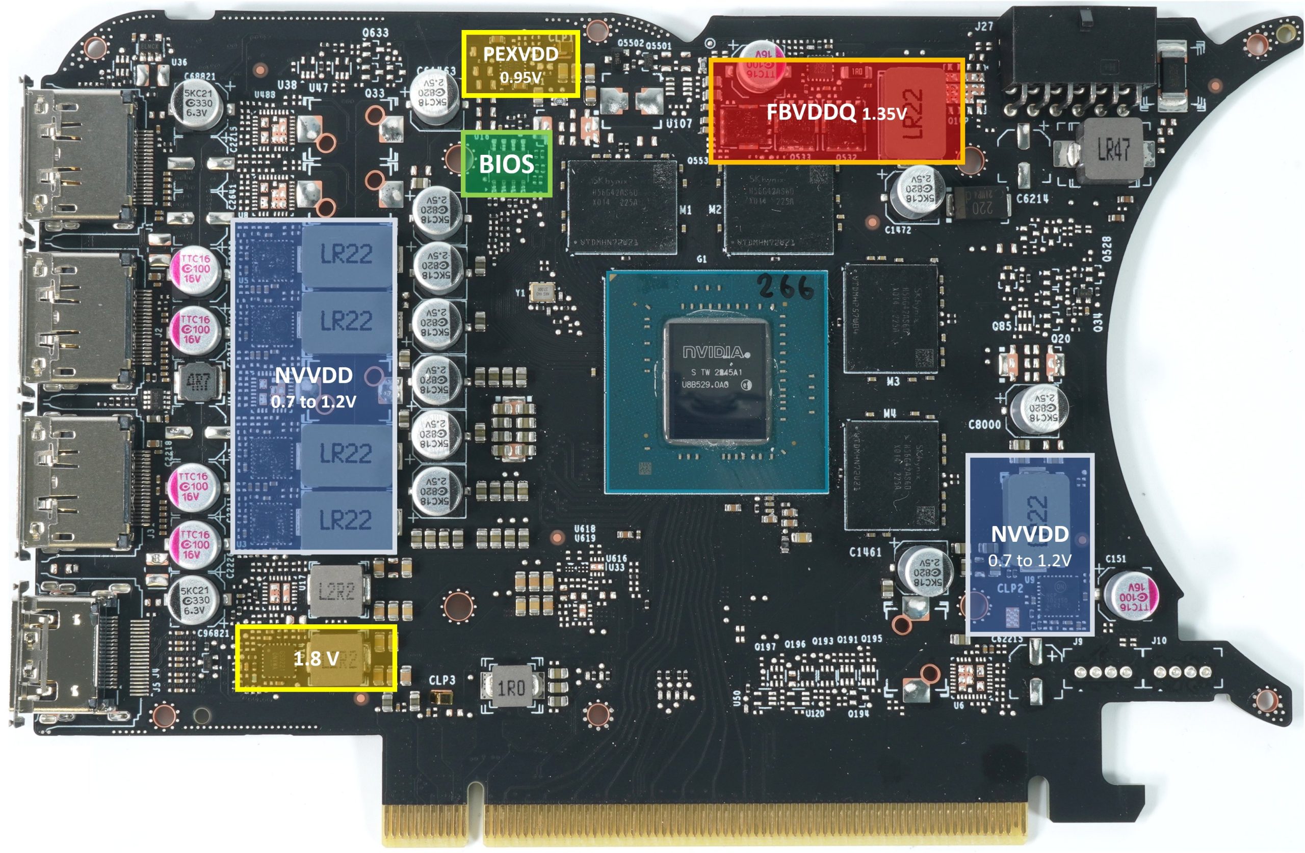
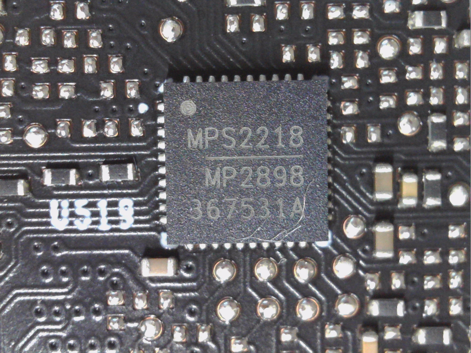
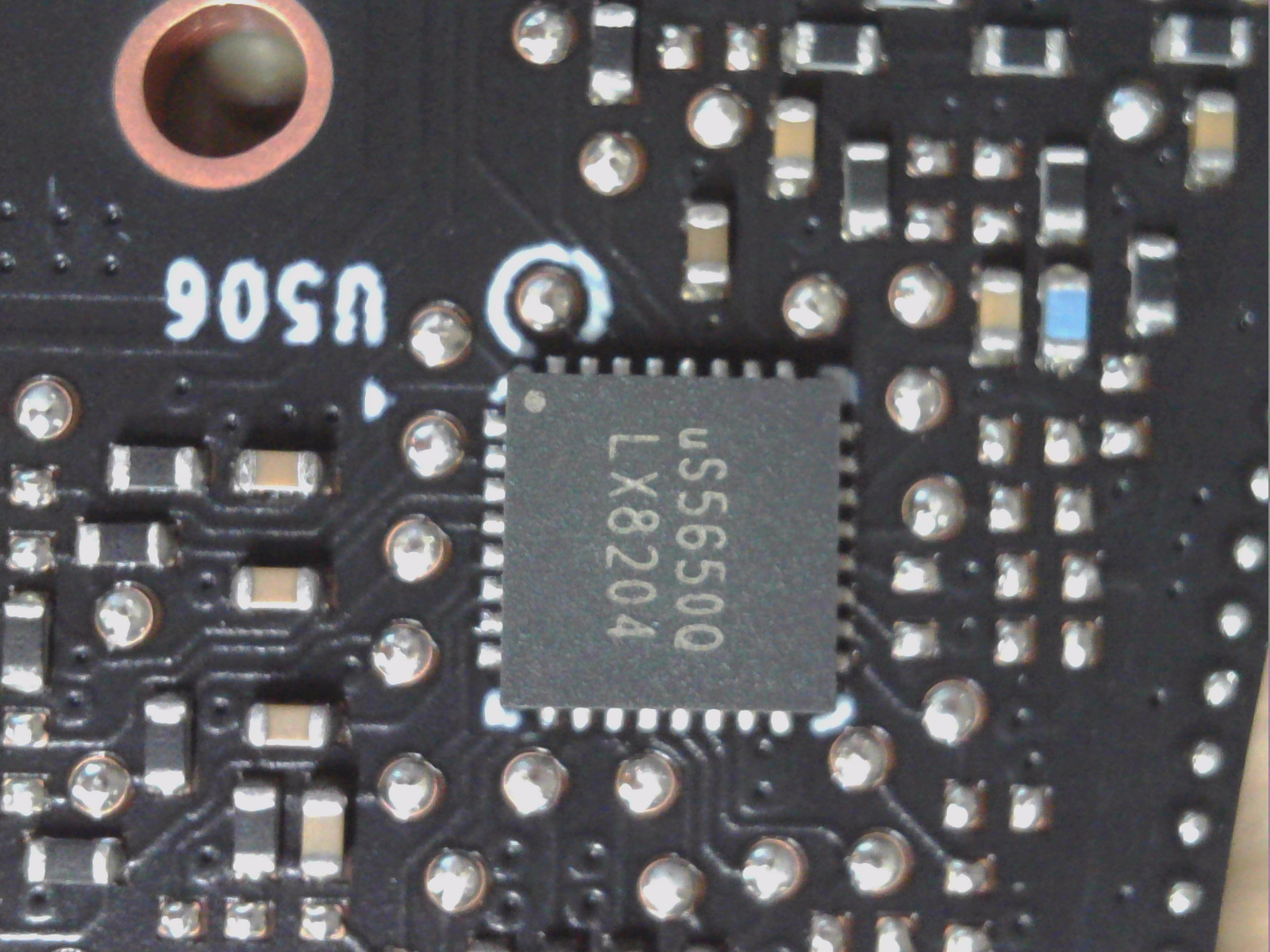
This all looks a bit too meager at first glance, but it’s enough. However, one again uses a common PWM controller for NVVDD (GPU core) and FBVDDQ (memory). And that’s why Monolith’s MP2898 is used for NVVDD, which is almost boring with the five phases on the first rail, but drives the one phase for the memory on the second rail. By the way, the controller is located on the back side of the board. On the other side there is a uPI uS5650Q for monitoring the four 12V rails (3x Aux and 1x PEG).
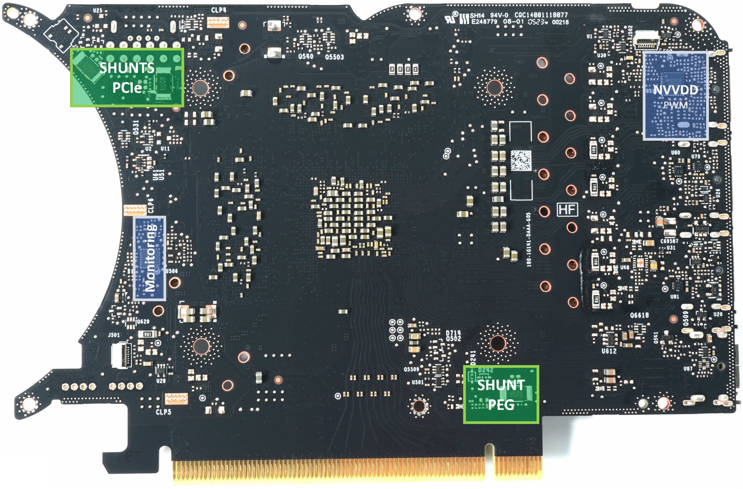
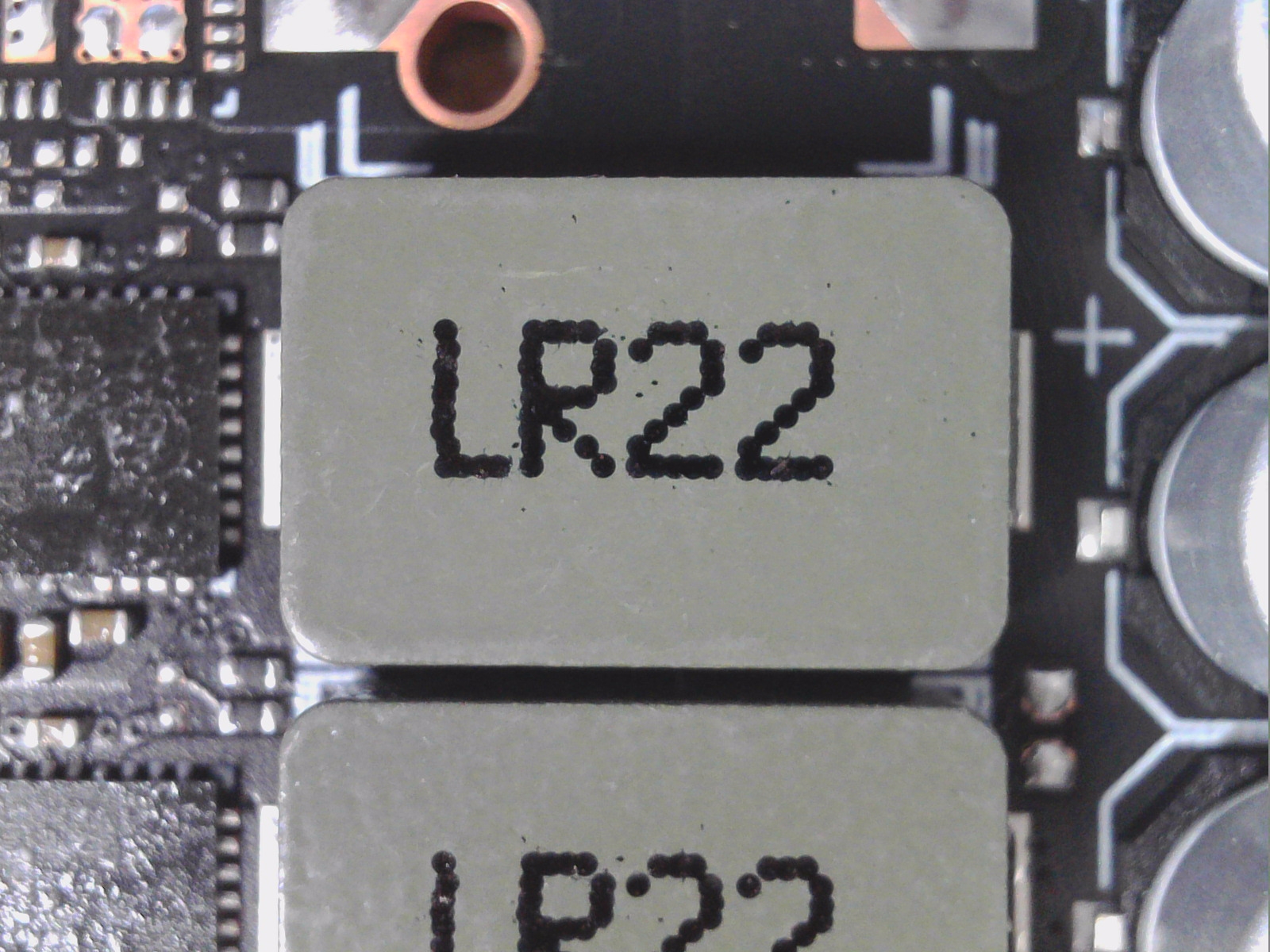
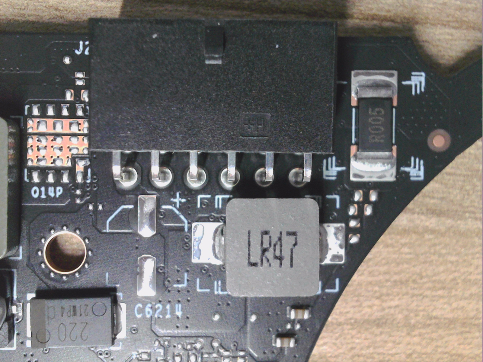
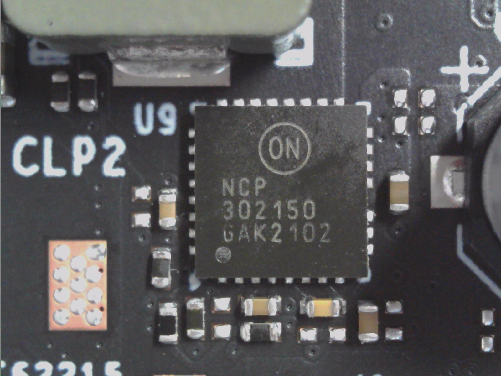
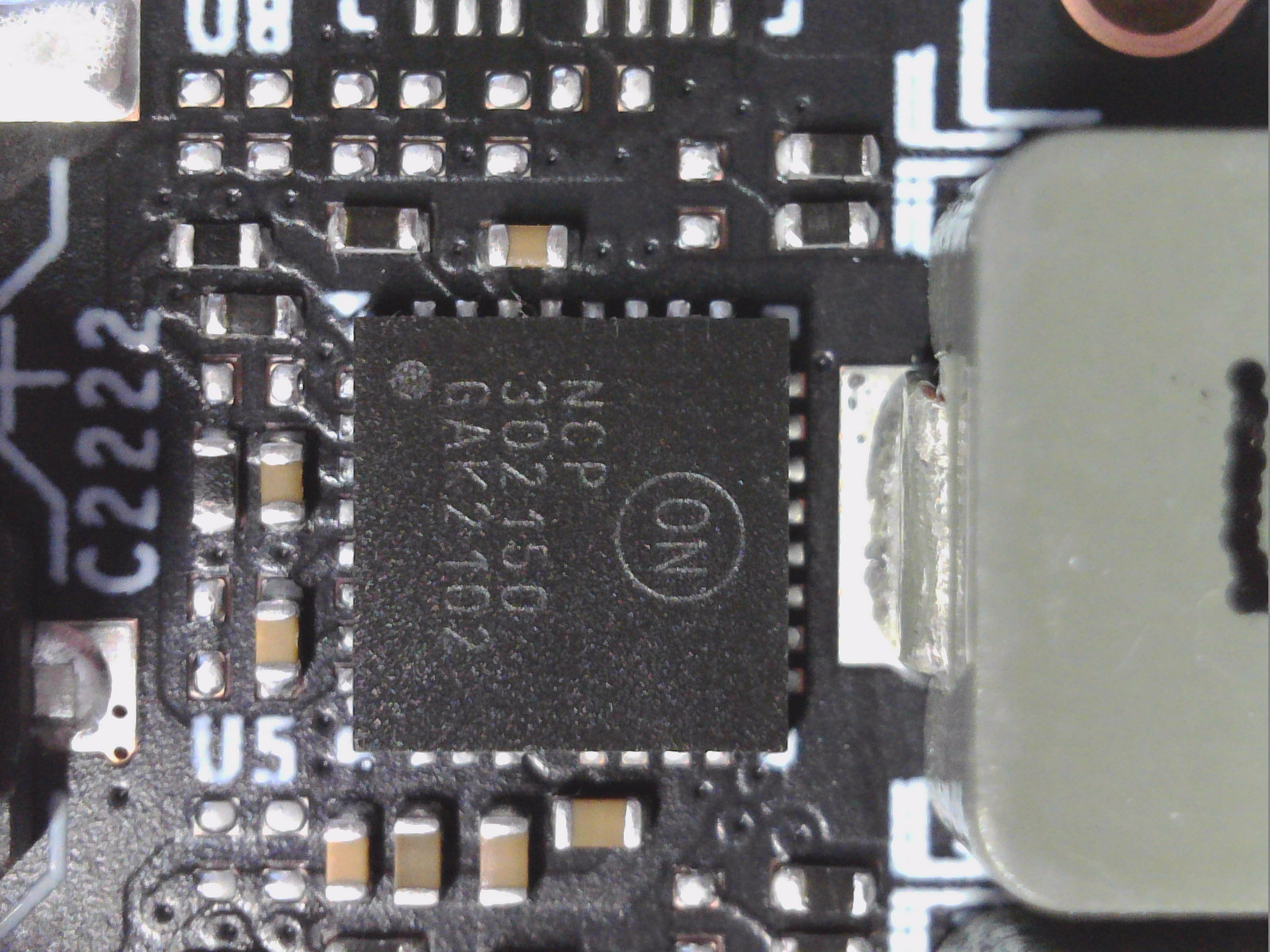
All used DrMOS for NVVDD are rather cheap products from OnSemi. The 50A peak current NPC302150 used in all control circuits for NVVDD integrates a MOSFET driver, a high-side MOSFET and low-side MOSFET in a single package. This chip is specifically designed for high-current applications such as DC-DC buck power conversion applications. This integrated solution reduces board space requirements compared to a discrete component solution. The coils used for NVVDD and the memory have an inductance of 220 nH, and the capacitors are in cup form, which is less expensive.
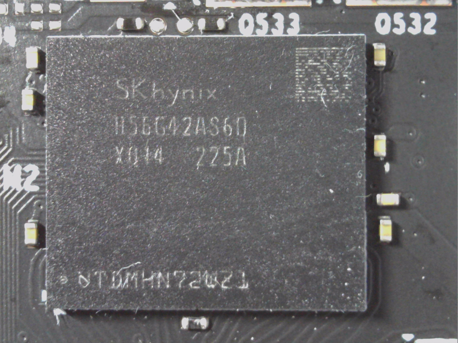
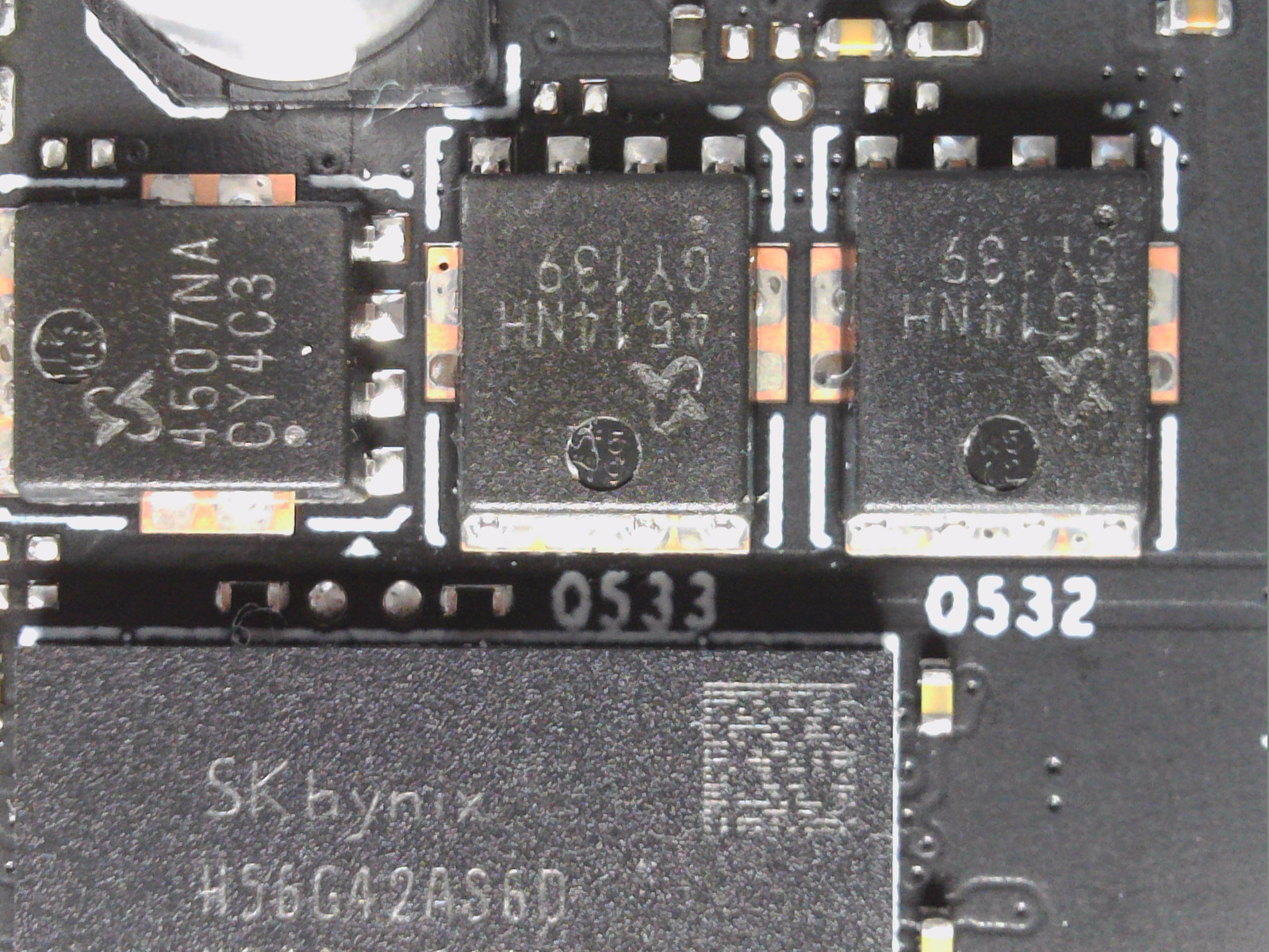
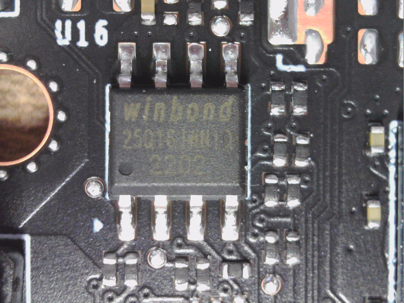
The one phase for FBVDDQ (memory) is realized discretely and consists on the high-side of an 4507 and on the low-side of two 4514 from Sinopower working in parallel. This is actually the lowest price drawer, but for the ample 10 watts of the memory still completely sufficient. The 12V rails on the 12+4 12VHPWR connector are combined into a single rail directly after the socket, another one is connected to the PEG and is only slightly used for NVVDD. The BIOS is in the usual place and the generation of the remaining extra-low voltages is as usual. So there are no more special features.

Teardown: The cooler
The magnetic back cover is set, of course, and disassembly has rarely been easier. Two lugs to hook onto the end of the card and a small snap mechanism on the slot panel are all that need to be used. The rest just clicks into place. The actual, firmly screwed backplate, which is also used for cooling, is then directly underneath. If you remove the screws, the board is exposed.
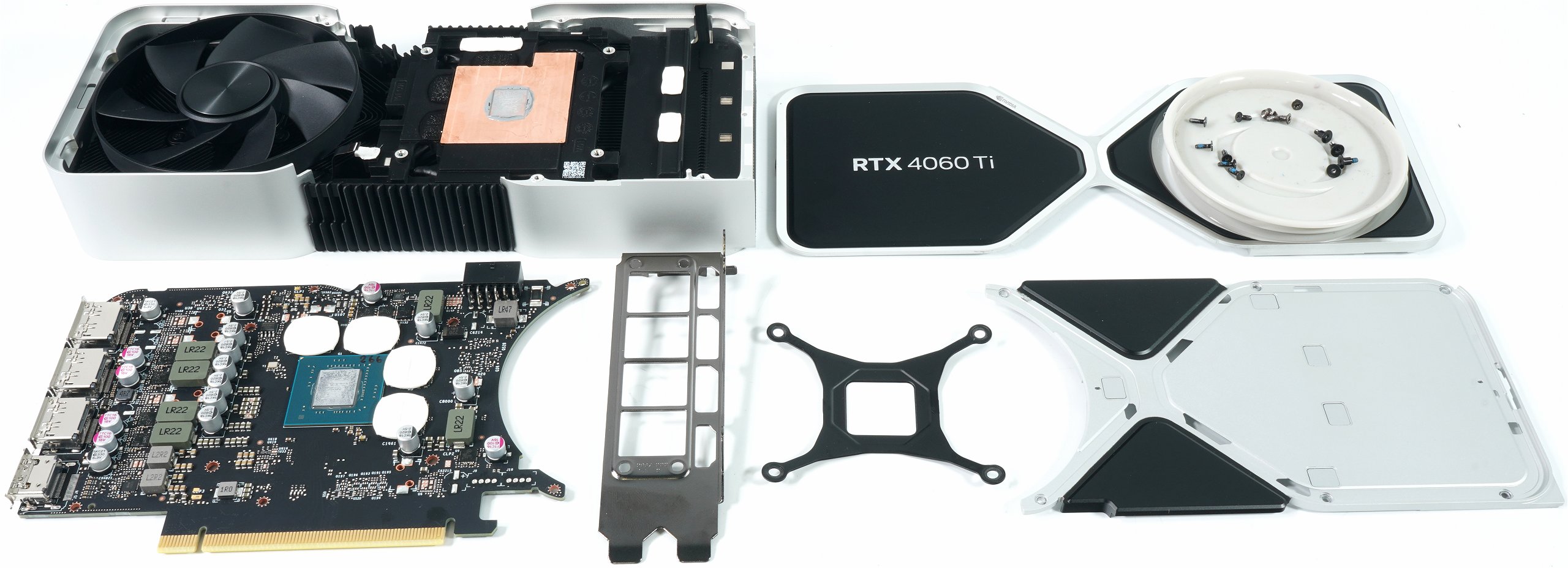
The rest is quickly explained. A solid copper heatsink is used instead of the usual vapor chambers and a total of four heatpipes.
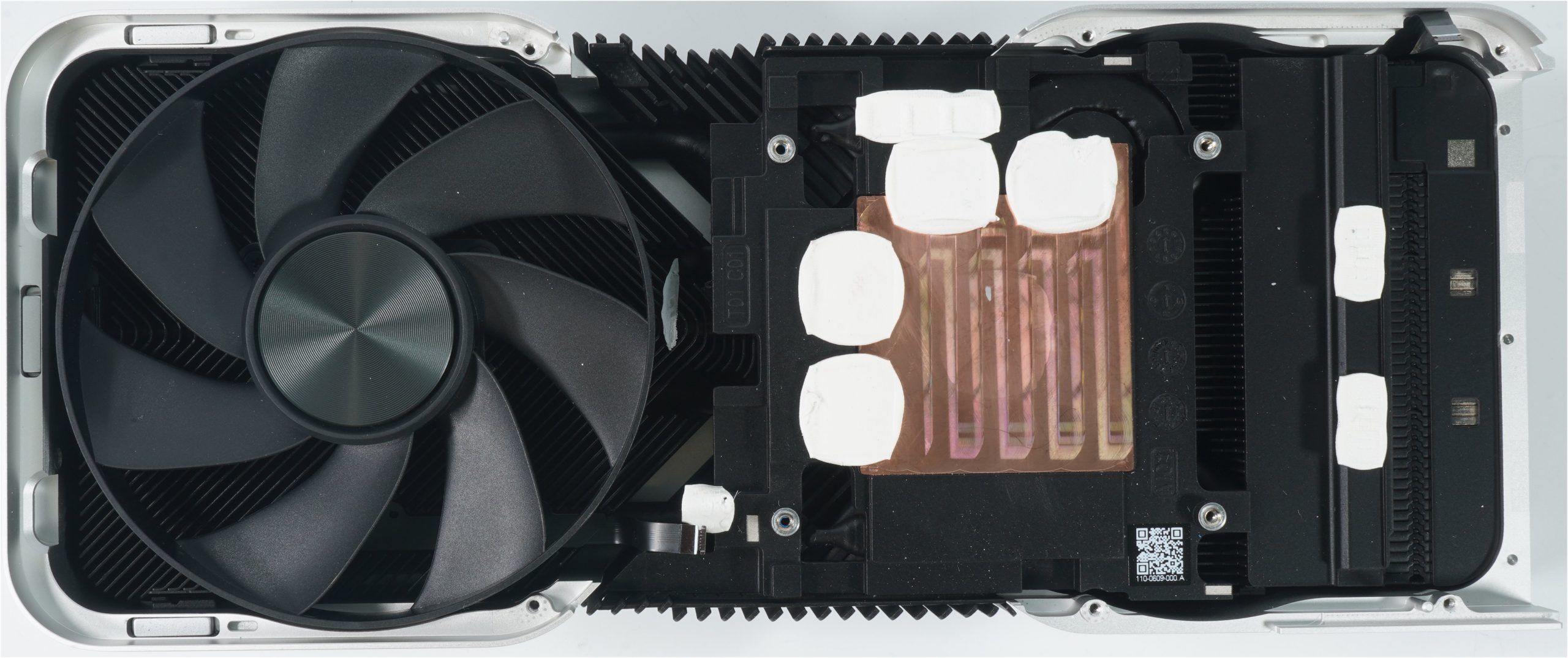
The pads used are in the style of the RTX 3080, ultra-soft and well-deformable, but not from the top shelf. So cost-down here as well. The inverse fan on the back has a rotor diameter of 9 cm and relies on seven rotor blades. The normally oriented fan on the front has a similar design.

- 1 - Introduction, technical data and technology
- 2 - The GeForce RTX 4060 Ti FE in detail
- 3 - Test System in the igor'sLAB MIFCOM-PC
- 4 - Teardown: PCB, components and cooler
- 5 - Gaming performance FHD (1920 x 1080)
- 6 - Gaming performance WQHD (2560 x 1440)
- 7 - Gaming performance DLSS vs. DLSS3 vs. FSR
- 8 - Latencies and DLSS 3.0
- 9 - Details: Power consumption and load balancing
- 10 - Load peaks, capping and PSU recommendation
- 11 - Temperatures, clock rate and thermal imaging
- 12 - Fan curves, noise level and audio samples
- 13 - Summary and conclusion


418 Antworten
Kommentar
Lade neue Kommentare
Urgestein
Moderator
1
Urgestein
1
Urgestein
Mitglied
Veteran
Veteran
1
Veteran
Veteran
Neuling
Mitglied
Mitglied
Urgestein
Mitglied
1
1
Alle Kommentare lesen unter igor´sLAB Community →