


Board analysis and power supply
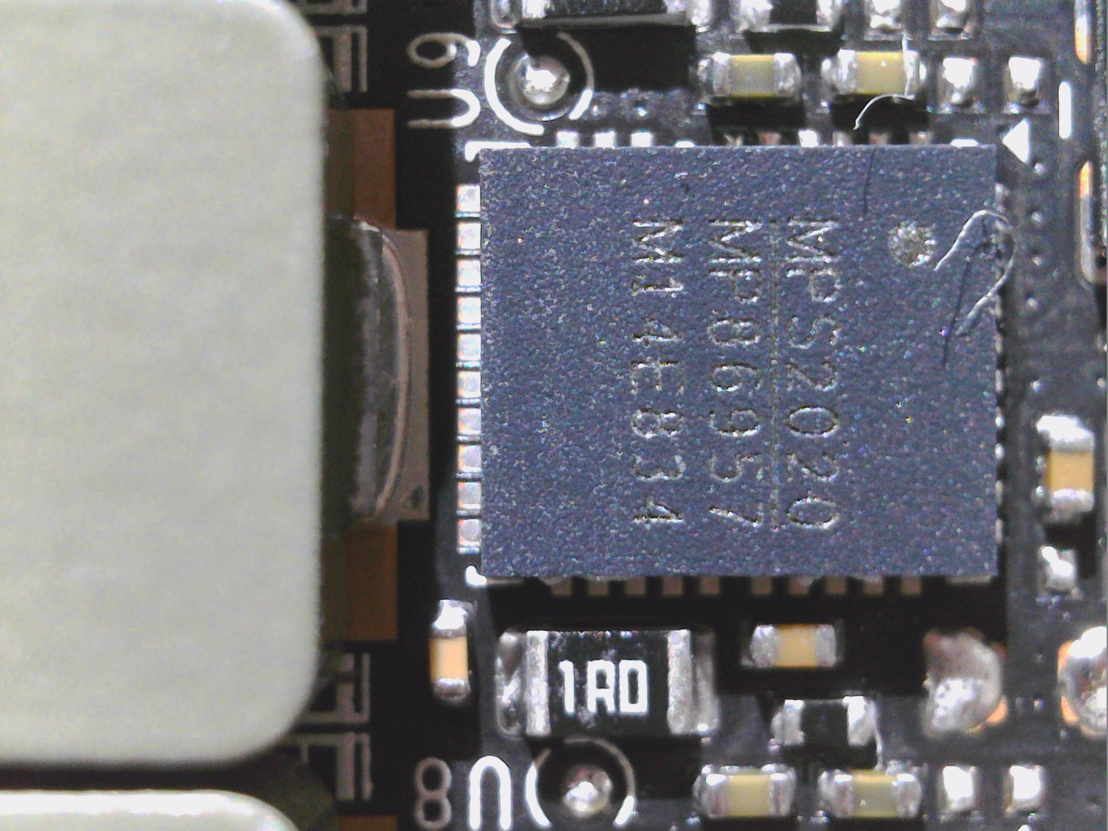
The board assembled at Foxconn has the 12-layer board with backdrill method which I mentioned several times. Also the type of power supply is new and I was also right with my assumptions. If we take a look at the upper side of the board, we immediately recognize the division of the main power supply. NVDD (blue) stands for the conventional core voltage, which is what we like to call GPU voltage. Here there are a total of nine individual phases, which are provided by a monolith MP2888A on the back (blue). This is a digital PWM controller with VID interface, compatible with NVIDIA’s Open VReg specification. The MP2888A can generate up to 10 phases. The nine phases are each implemented with still very sparsely documented Smart Power Stages (PLC) MP86957 from the same manufacturer, which also enable MOSFET DCR.
The assembly of the power supply MSVDD (green), which I had called “Gedönsspannung” and which stands for “Miscellaneous”, is similar. We find a total of six individually controlled phases generated by a MP2886B from Monolith (back, green), the little brother of the MP2888A from just now. The six PLCs again rely on the MP85957 from the same manufacturer. In the end, there are 15 phases for the GPU alone and the various voltages for it. This should also make power gating in the GPU a bit easier, although AMD uses a similar, if much smaller, outsourcing with VDDCI.
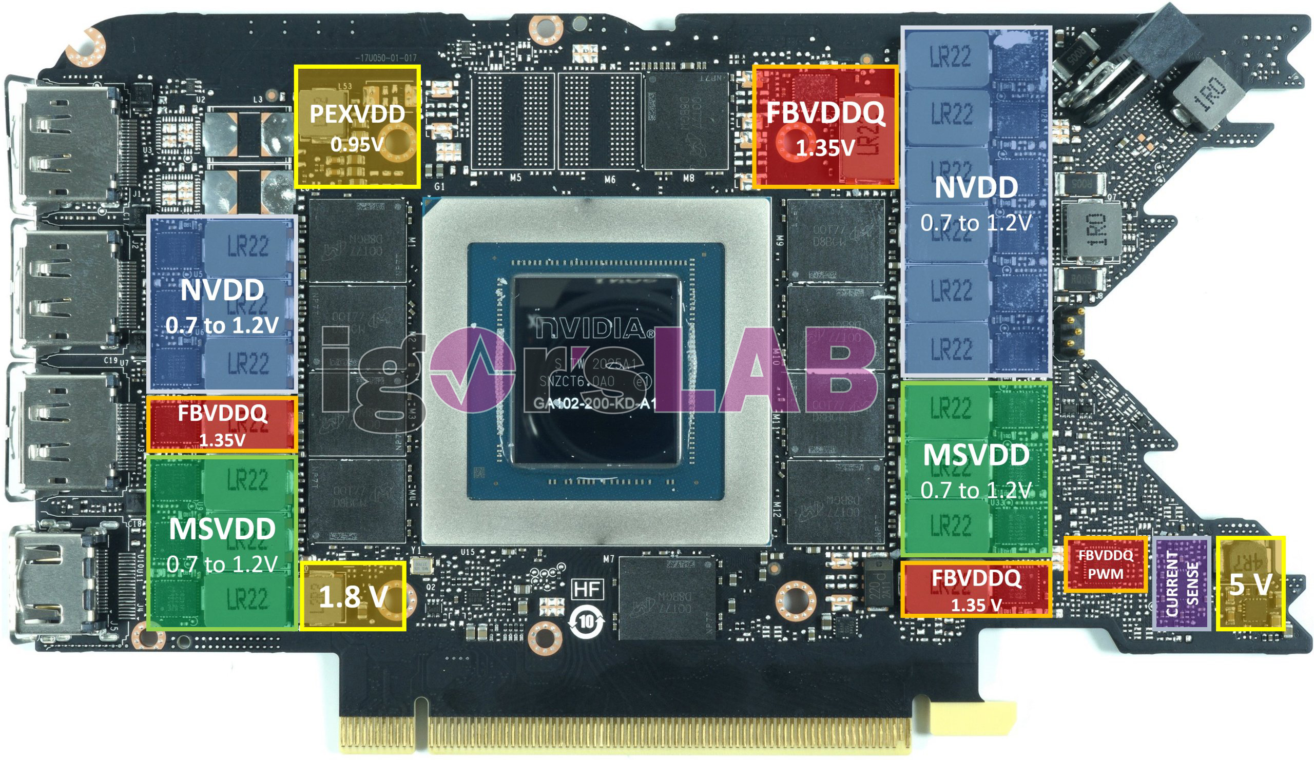
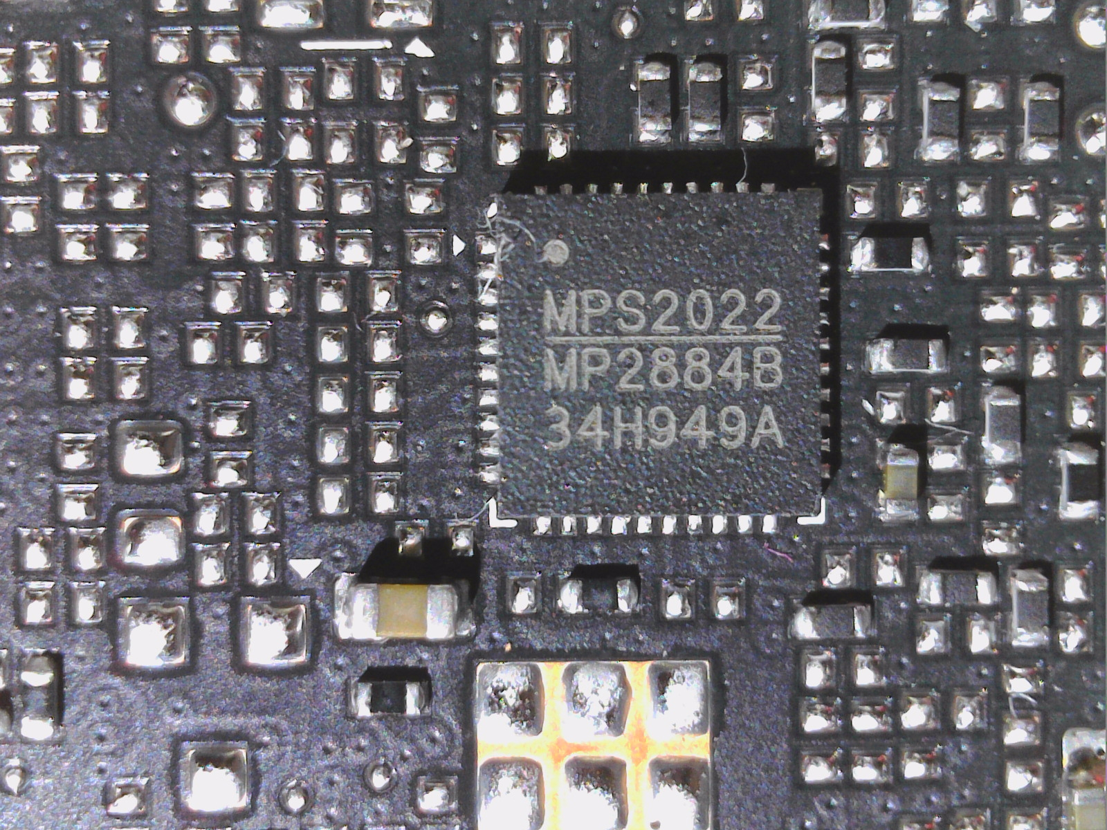
NVIDIA uses three phases for the memory, which are generated by an even further reduced MP2884B from Monolith, whereby the PLCs are of the same type as the previous ones. However, the PWM controller is located on the front side The PLC of the PCI Express voltage PEXVDD and the 1.8 Volt are also located on the rear side, the corresponding coils on the front side. There you will also find a 5V-conditioning on the bottom right.
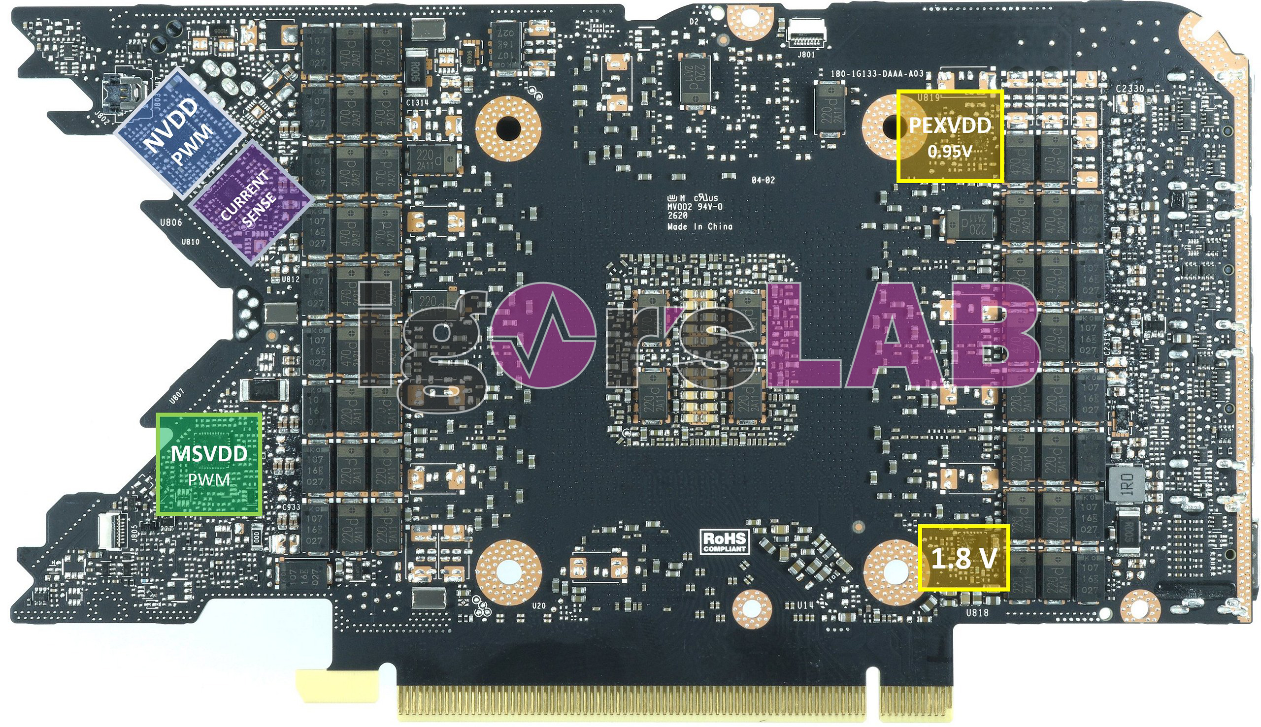
For input smoothing, three coils with 1 µF each are used, behind which a shunt is located, over whose voltage drop the flowing currents are measured. However, since the firmware can also evaluate the MOSFET DCR of the PLC, shunt mods are no longer so easily possible. On the right side we see the big PWM controller MP2880A from Monolith for NVDD on the back.
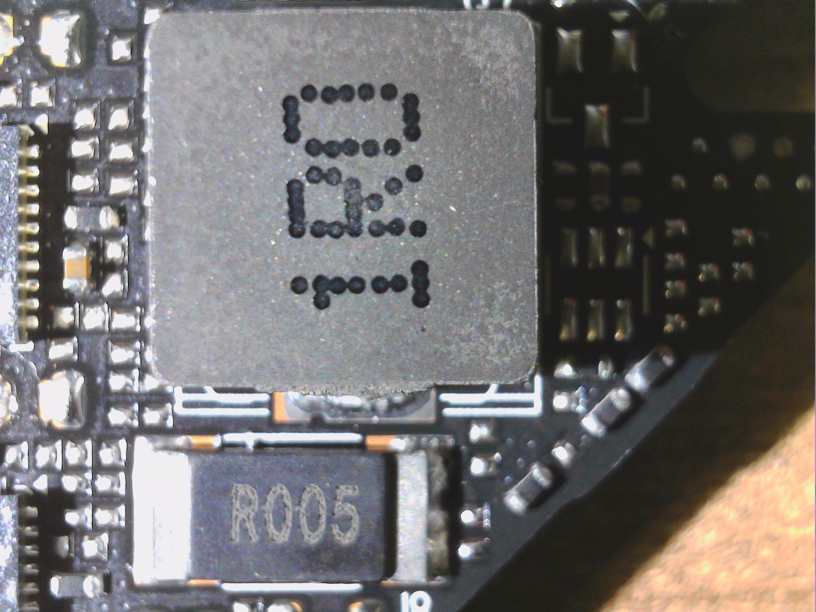
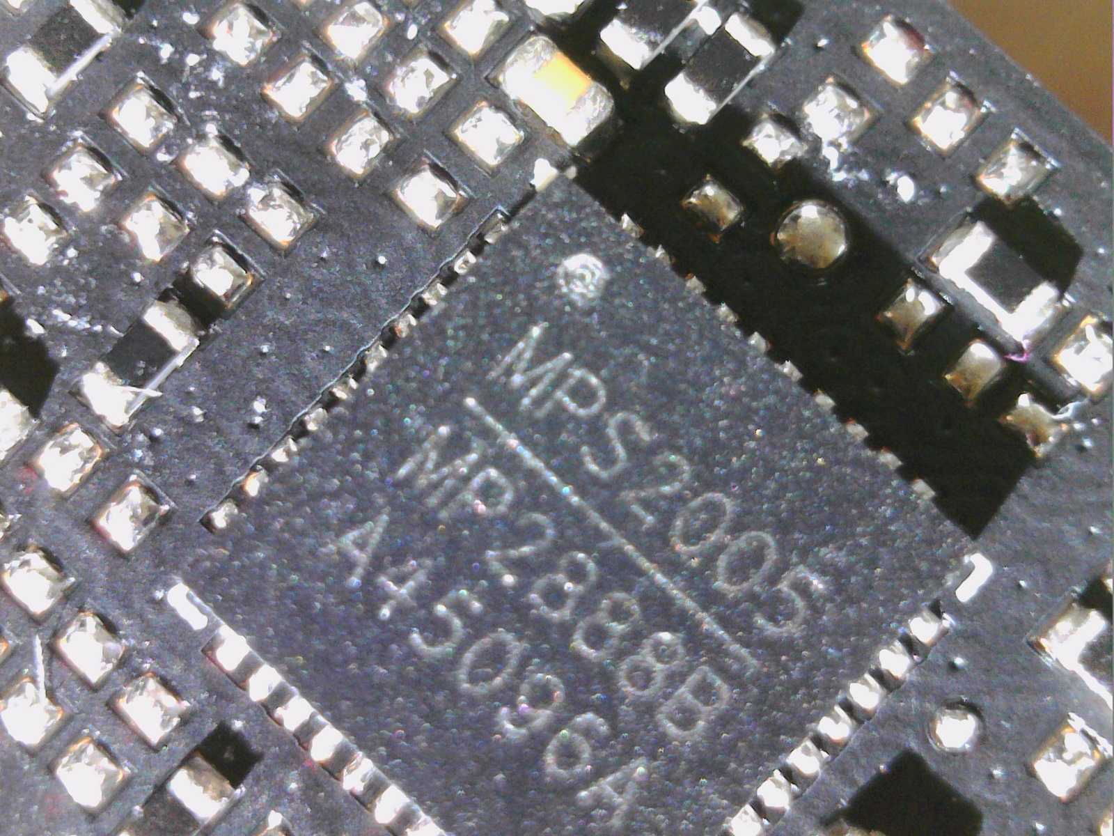
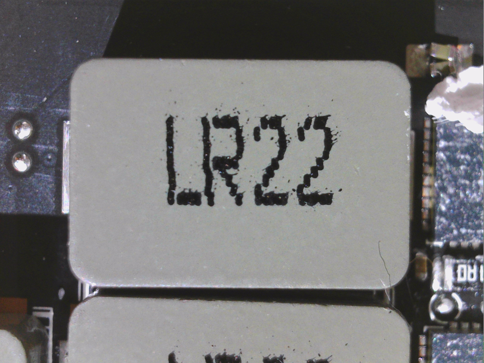
The following two pictures show one of the MP86957 Power Stages, which is used in all three large supply circuits, and one of the many 220 mH coils as an example for all PLCs. The MP2880A for MSVDD is not shown here, because it looks not much different from the MP2884B of the memory.
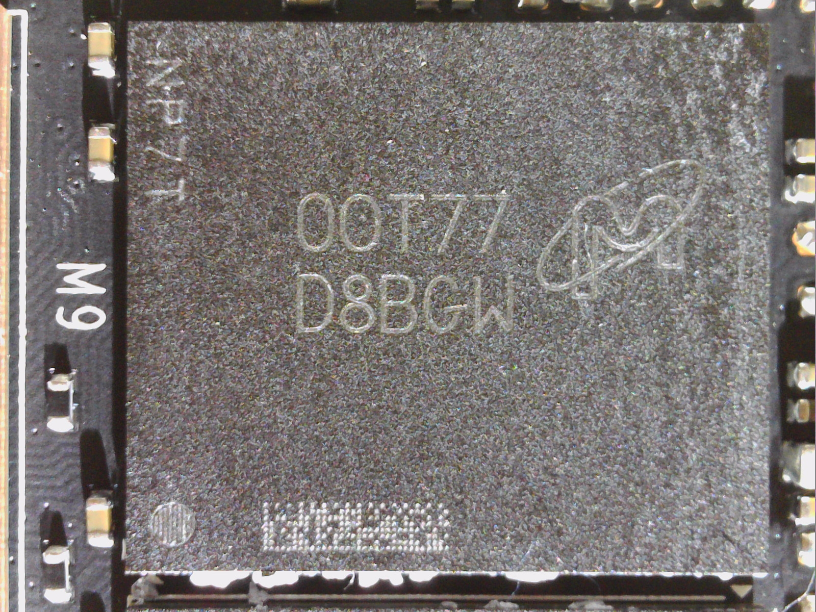
We see below the MP2884B for the memory and one of the memory modules from Micron. The total of ten 1 GB modules of the GDDR6X memory come from Micron. The memory runs at only 19 Gb/s, although it could actually run at 21 Gb/s. The extent to which NVIDIA wanted to prevent thermal problems here can of course only be speculated.
Cooler and disassembly
The disassembling of the cooler is quite tricky, here I like to refer to the appropriate video, which I will upload bilingually. The body is mainly made of light metal with a quite clever surface, which also made me think of a plastic coated with metal powder when I was unboxing because of the “GEFORCE RTX” lettering. The actual cooler is multi-part and consists of an efficient, nickel-plated heat sink. Four flattened heatpipes are soldered to the back of the heat sink, which then extend longitudinally to the end of the card.
Two PWM-controlled 8.5 cm fans with a very interesting rotor blade geometry, almost reminiscent of the design of radial fans, sit above the heatsink and the open structure. Well, almost. But also the maximum speed of the two separately controlled fans of up to 3500 rpm is not exactly an expression of noble reserve. Let’s hope it stays quieter here than the map could if it had to.
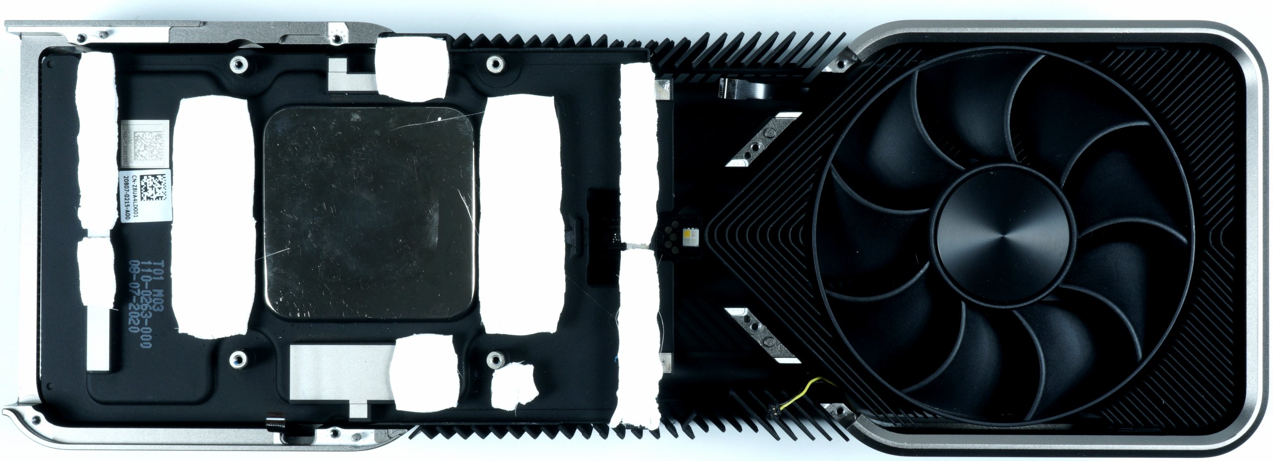
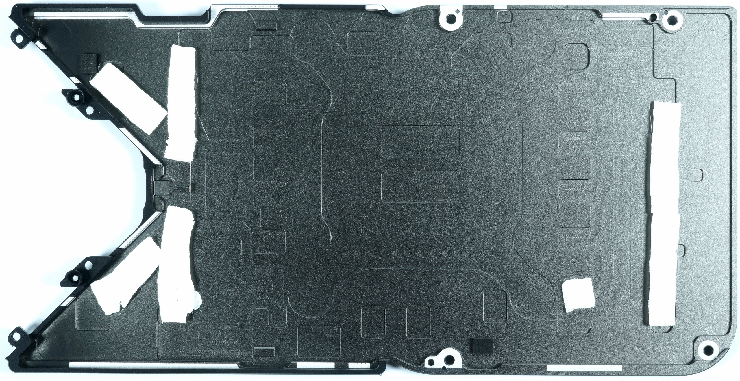
The backplate is also made of light metal, which has a matt black coating on the outside. The manufacturer thermally connects only the voltage converters and the PWM controllers to the backplate. The areas under the memory and the BGA remain at the back without cooling.
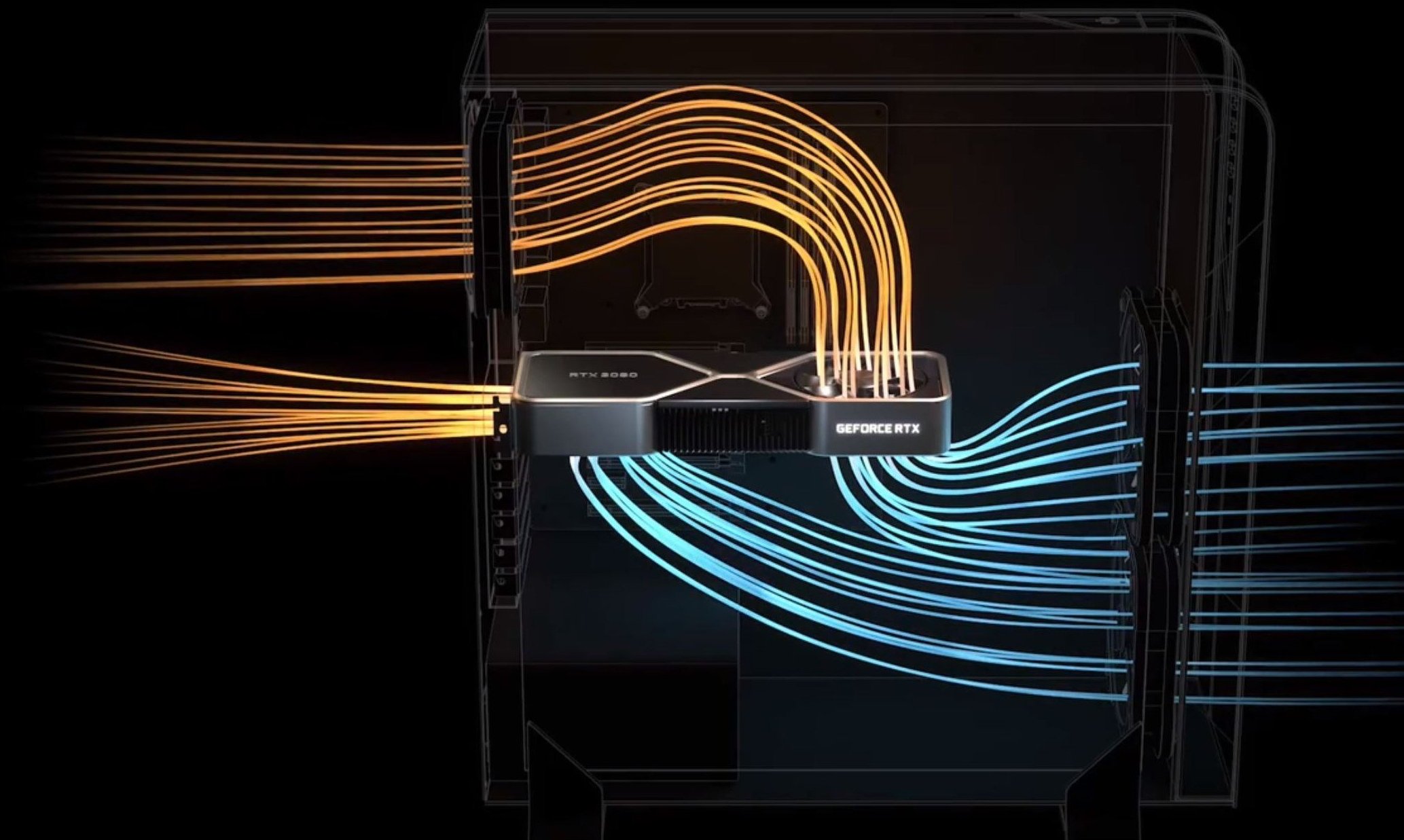
There has already been a lot of speculation about the principle with the different suction and blowing directions, so I won’t repeat myself but only try the foil again. We will see the test in the closed housing anyway.
- 1 - Introduction, Unboxing and Test System
- 2 - Teardown, PCB analysis and Cooler
- 3 - Gaming Performance: WQHD and Full-HD with RTX On
- 4 - Gaming Performance: Ultra-HD with and without DLSS
- 5 - FPS, Percentiles, Frame Time & Variances
- 6 - Frame Times vs. Power Comsumption
- 7 - Workstation: CAD
- 8 - Studio: Rendering
- 9 - Studio: Video & Picture Editing
- 10 - Power Consumption: GPU and CPU in all Games
- 11 - Power Consumption: Efficiency in Detail
- 12 - Power Consumption: Summary, Transient Analysis and PSU Recomendation
- 13 - Temperatures and Thermal Imaging
- 14 - Noise and Sound Analysis
- 15 - NVIDIA Broadcast - more than a Gimmick?
- 16 - Summary, Conlusion and Verdict


Kommentieren