


TU102 – The Grand-Turing
The TU102 chip at the heart of the GeForce RTX 2080 Ti is huge with its 754 square millimeters. Its 18.6 billion transistors are realized with TSMC's 12nm FinFET manufacturing process, which is said to provide a slight density improvement over TSMC's previous 16nm process. TSMC presents the 12nm technology under the same heading as the 16nm technology on its own website. Why anytime.
The fact that Nvidia's "large" gaming GPU is being introduced at the same time as a new architecture is new. But Nvidia knows full well that real-time ray tracing needs to run smoothly to really inspire enthusiasts with the new technology. Publishing the TU102 as early as possible was therefore only logical. Compared to the GP102, the largest Pascal-based GPU currently used in a desktop graphics card, Nvidia's TU102 is now a whopping 60% larger and has a 55% higher number of transistors. But it's still not the company's largest graphics processor.
The Turing flagship is even dwarfed by the "old" GV100, a 21.1 billion transistor giant with a size of 815 mm2. Launched in 2017, this GPU focused on data center applications and is still found on the extremely expensive Titan V. However, the TU102 is aimed at a completely different target group than the GV100 and therefore also has a number of other features. While parts of Turing are based on the GV100, other parts of the Volta architecture that either don't benefit players or aren't cheap to manufacture on the desktop have been deliberately removed.
For example, each streaming multiprocessor (SM) of Volta contains 32 FP64 cores for fast double-precision calculations, which adds up to 2688 FP64 cores in the GV100. However, these are not really useful in normal games and they devour a lot of space in return, leaving Nvidia with only two per SM. As a result, the TU102's double precision rate is only 1/32 of its FP32 power. This provides just as much FP64 compute power to maintain compatibility with the software that depends on it.
Similarly, the GV100's eight 512-bit memory controllers connected to four stacks of the HBM2 would have been far too expensive. Here Nvidia will surely have also looked to AMD and noticed the difficulties that one had there to produce the Radeons with HBM2 assembly still reasonably cost-covering (or not). The HBM2 has therefore been replaced by GDDR6, which allows for a much more cost-effective solution that is still able to perform a large bandwidth upgrade over Pascal-based predecessors and where module availability is also significantly higher Should.

A complete TU102 graphics processor consists of six Graphics Processing Clusters (GPCs), each consisting of a raster engine and six texture processing clusters (TPCs). Each TPC consists of a PolyMorph (Fixed-Function Geometry Pipeline) engine and two streaming multiprocessors (SMs). At the SM level, we find 64 CUDA cores, eight tensor cores, one RT core, four texture units, 16 load/storage units, 256KB register file storage, four L0 statement caches, and a 96KB configurable L1 cache/shared storage structure.
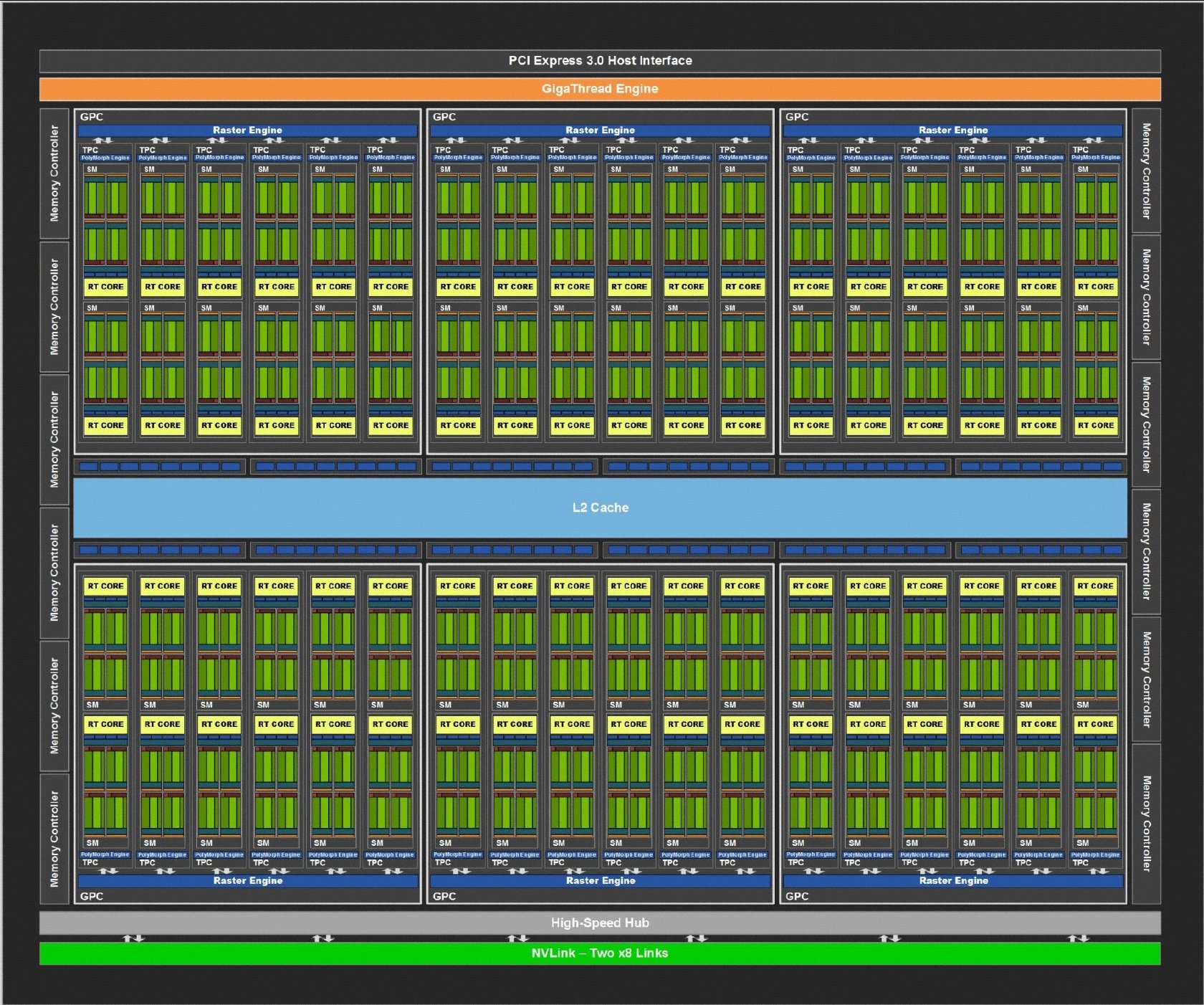
Multiplyall of this, you get a graphics processor with 72 SMs, 4608 CUDA cores, 576 tensor cores, 72 RT cores, 288 texture units and 36 PolyMorph engines. This construct is powered by twelve 32-bit GDDR6 storage controllers, each connected to an 8-ROP cluster and 512KB L2 cache, resulting in an aggregated 384-bit storage bus, 96 ROPs, and a 6 MB L2 cache. Reads a lot and it is.
All composite: GeForce RTX 2080 Ti
However, the TU102 on the GeForce RTX 2080 Ti is not a fully developed processor. Whether Nvidia wanted to leave room for a Titan-class model in addition to the Quadro RTX 8000, or whether the yields of fully functional GPUs from a certain bin were no longer satisfactory– the RTX 2080 Ti disables two of the TPCs, which is then shown in a card with 4352 CUDA cores, 544 tensor cores, 68 RT cores, 544 texture units and 34 PolyMorph machines.
In addition, one of the TU102's 32-bit storage controllers is shut down, creating an aggregated 352-bit bus that transmits the data to 88 ROPs and 5.5 MB l2 cache. Nvidia adapts its strategically equipped GPU to Micron's MT61K256M32JE-14:A memory modules. Eleven of these modules sit on the PCB of the GeForce RTX 2080 Ti and thus logically one space remains available. Nevertheless, the theoretical peak bandwidth increases sharply compared to the previous generation due to the higher data rate of the GDDR6: at 14 Gb/s on a 352-bit interface it is 616 GB/s. In comparison, the 11Gb/s GDDR5X on the GeForce GTX 1080 Ti delivered only 484GB/s.
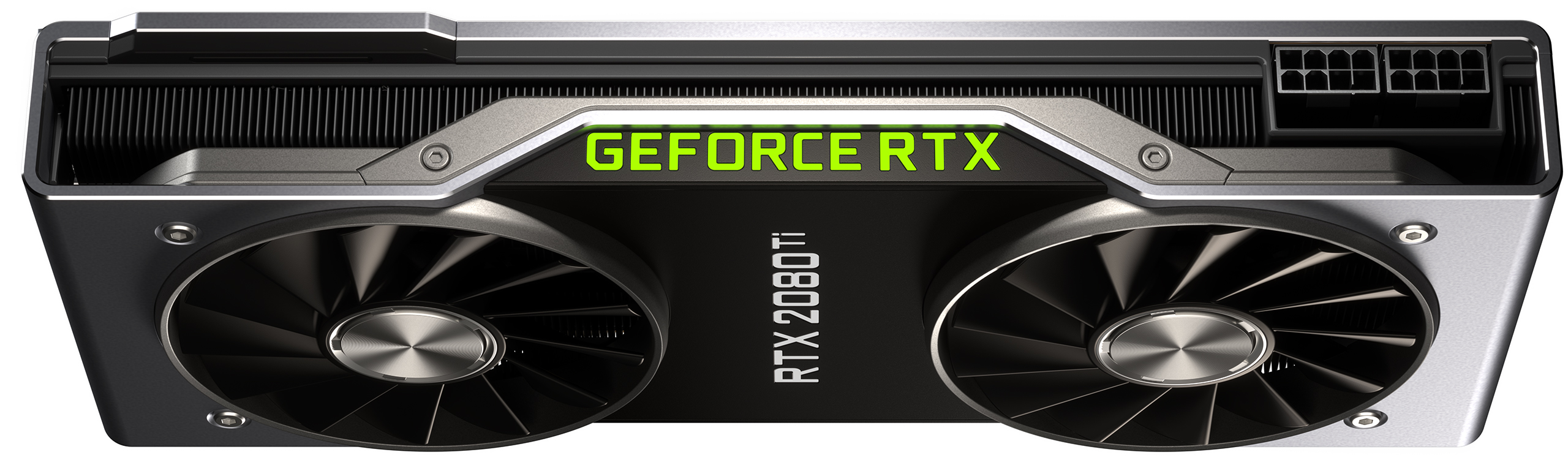
At least on the Founders Edition card, the base clock can jump from 1350 MHz to a typical GPU boost rate of 1635 MHz as long as the GeForce RTX 2080 Ti runs cool enough. And because Nvidia provides maximum compute performance with GPU boost-based numbers, the top-end model achieves up to 14.2 TFLOPS single-precision performance. The reference specification provides for a typical GPU boost frequency of 1545 MHz and a slightly lower TDP. While the Overclocking of the Founders Edition card provides for a maximum board power (TBP) of 260W, the reference cards should be around 250W.
- 1 - Einführung und Vorstellung
- 2 - TU102 + GeForce RTX 2080 Ti
- 3 - TU104 + GeForce RTX 2080
- 4 - TU106 + GeForce RTX 2070
- 5 - Performance-Anstieg für bestehende Anwendungen
- 6 - Tensor-Kerne und DLSS
- 7 - Ray Tracing in Echtzeit
- 8 - NVLink: als Brücke wohin?
- 9 - RTX-OPs: wir rechnen nach
- 10 - Shading-Verbesserungen
- 11 - Anschlüsse und Video
- 12 - 1-Klick-Übertaktung
- 13 - Tschüss, Gebläselüfter!
- 14 - Zusammenfassung und Fazit


Kommentieren