


With the GeForce RTX 2080 Ti, Nvidia has reached deep into the trick box in the board layout and especially in the power supply. In the theory article I have already written something about the changed power supply, here I go into more detail. We count three phases for memory and also see the appropriate PWM controller on the front. I will discuss the exact components of the entire board in more detail.
But stop, what is that? If you now count the remaining voltage transformer circles, you get to 13 pieces. However, since there is no PWM controller that could realize this (why?), six double phases remained to get to 12 circles. But it doesn't fit either. This would only be possible with the 13 if one of the voltage converter circles had been split up again as a load balancer, which would not make sense as a 6 x 2 + 1.
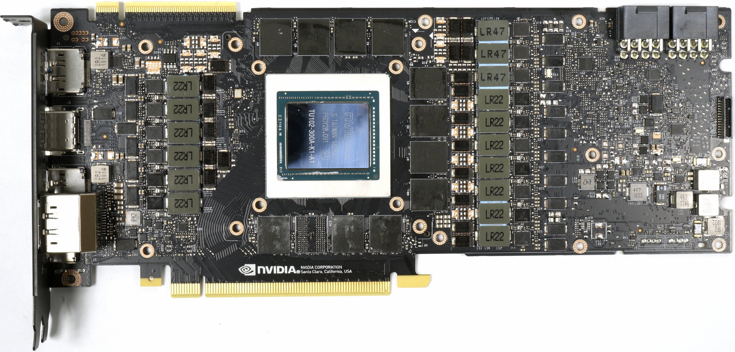
Then one wonders what exactly is there. If you look at the board, the result is more than unusual, but smart. On the back is the same PWM controller again, but this time for the eight GPU phases. You read correctly, it's eight phases! 5 phases are fed from the two PCIe connectors and doubled each. With two control circuits per phase, you can then get 5 x 2 to 10 voltage converter circuits.
The remaining three phases, which are located on the upper image to the left of the GPU, are fed from the motherboard slot (PEG) and are not doubled! This is how you end up with the 13, which also enables a very smart load distribution in this way. A bit tricky, but that's kind of tricky. In order to be able to implement all this well, you also need the right components. And that's exactly what I'm coming to right now.
By the way, you can see from the front and back how tightly the board is equipped and how Nvidia has nevertheless managed to distribute the thermal hotspots sensibly.
Power supply of the GPU
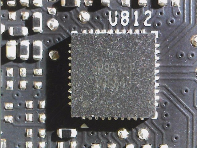
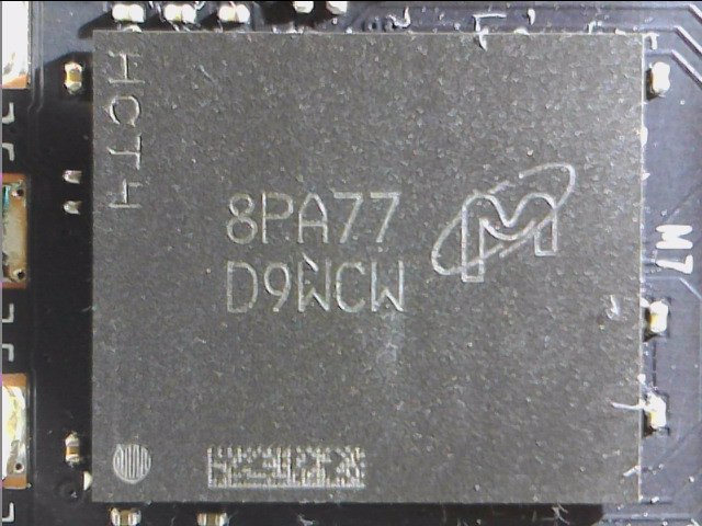
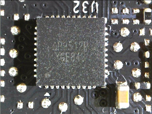
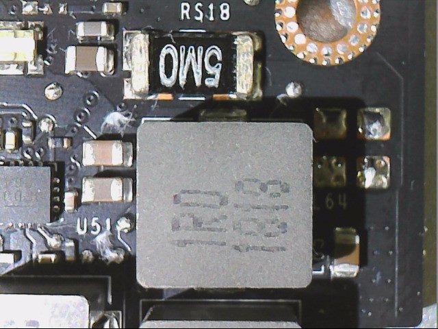
Let's start with the most interesting part! The quite new uP9512 on the back is used here as an 8-phase PWM controller, which has been specially developed for the provision of high-precision output voltage systems for the latest generation of GPUs. The uP9512 has programmable output voltage and active voltage positioning functions to adjust the output voltage depending on the load current, so that it is optimally positioned for a good load current transition.
The uP9512 supports NVIDIA Open Voltage Regulator Type 4i+ with PWMVID function. The PWMVID input is buffered and filtered to create a very accurate reference voltage. The output voltage is then precisely controlled on the reference input. The integrated SMBus interface offers enough flexibility to optimize performance and efficiency and also to connect the appropriate software. The controller also supports new Smart Power Stage chips (PLCs). Appropriate PLC then provide very accurate information about e.g. currents (IMON) and temperatures (TMON).
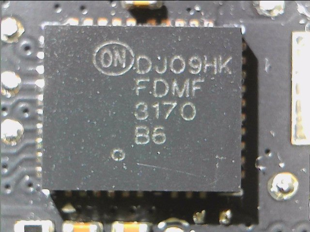
An important feature is also the flexible hardware specification to adjust the operating phase number in different load current states. In addition, soft start to avoid peaks, channel current limitation, undervoltage protection, overvoltage protection and power good output. And because we are in the process, we are coming straight to the Plc. All 13 voltage converter circuits are equipped with the FDMF 3170 from ON Semiconductor, a PowerTrench® MOSFET and equivalent to the original Fairchild, which I had already seen on an evaluation board of an AIC.
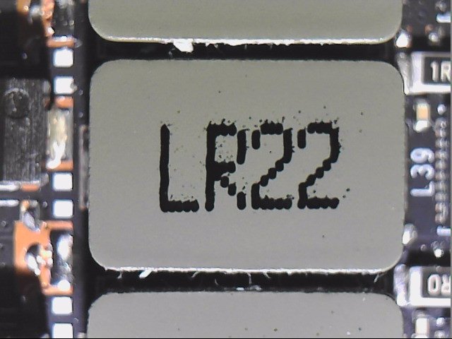
In the case of coils, the usual encapsulated ferrite core coils are used, but this time they are rectangular in order to create more space for the high number of voltage converter circles with the narrower sides in the vertical row of the coils.
Power supply of the memory
The label on the memory identifies it as Micron's MT61K256M32. These are 8GB GDDR6 SGRAM modules (2 channels x 256 Meg x 16 I/O, 2 channels x 512 Meg x 8 I/O) with a bandwidth of 14Gb/s. Since a total of eleven modules are installed (the twelfth remains free), the well-known memory expansion of 11 GB also results.
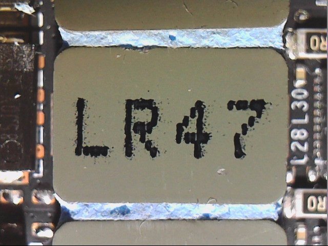
The three phases of the voltage converters, like the GPU, are provided by an uP9512 in a three-phase layout. The three FDMF 3170s also use the same PLC. The coils are slightly larger at 470 mH in the inductance, but are completely identical in terms of external dimensions.

Other details
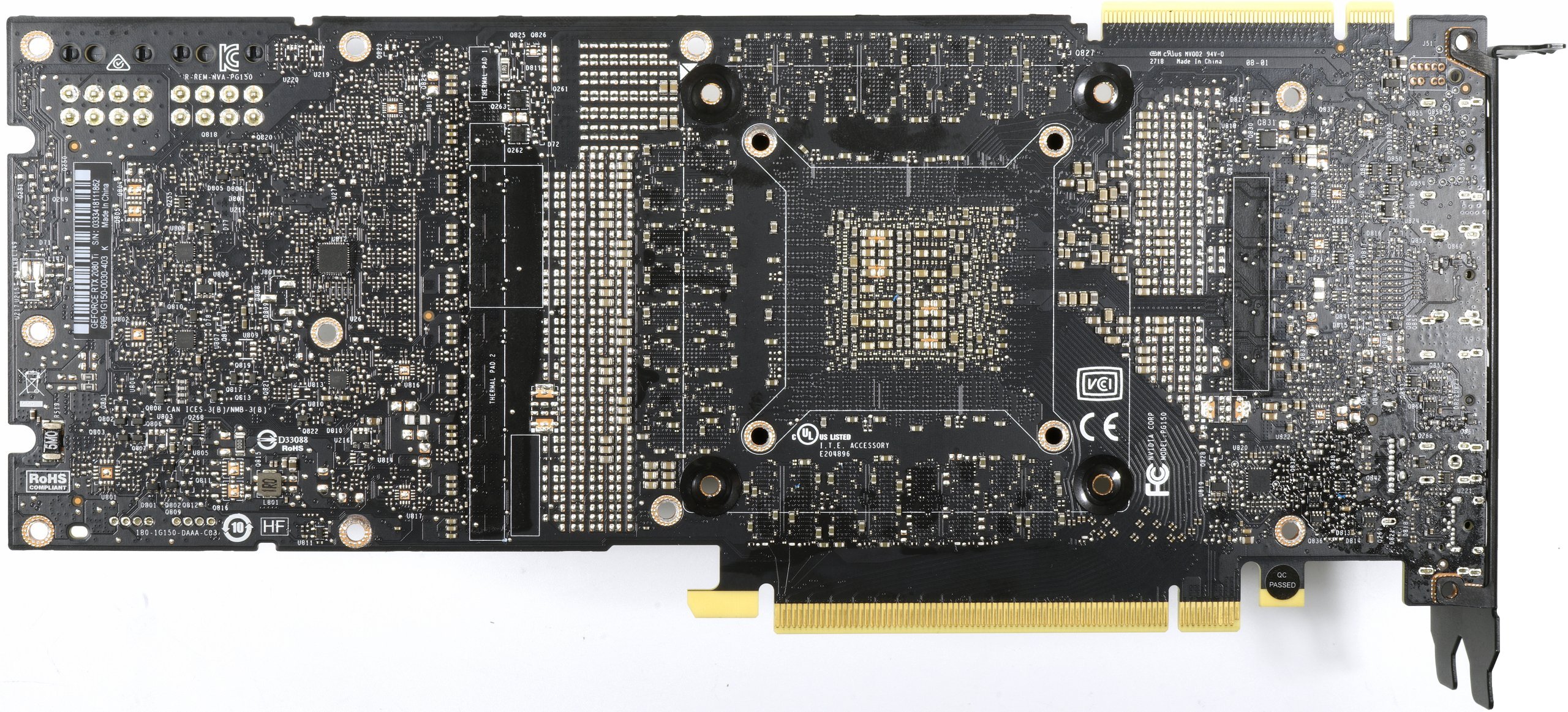
The input filtering is carried out via three 1-H coils, wherein there is a suitable shunt in each of the three connection lines. This is a very low-impedance resistance to which the voltage drop is measured in parallel and passed on to telemetry. Thus, the board power can be limited quite exactly to what the manufacturer as a frame for the total power consumption or specified the respective supply line. The Silver Pencil faction will surely shrug nervously.
By the way, one of the shunts is on the back of the board. The card has only one single BIOS. It's a pity, but you can't have everything. Thus, we also search for the switch in vain. There is, logically, none.

This would have dealt with the most important thing about the board of the GeForce RTX 2080 Ti FE.
- 1 - Einführung, Unboxing, Daten
- 2 - RTX 2080 Ti - Platinenanalyse
- 3 - RTX 2080 - Platinenanalyse
- 4 - Raytracing in Echtzeit
- 5 - Deep Learning Super Sampling (DLSS)
- 6 - High Dynamic Range (HDR)
- 7 - Ashes of the Singularity: Escalation (DX12)
- 8 - Battlefield 1 (DX12)
- 9 - Destiny 2 (DX11)
- 10 - Doom (Vulkan)
- 11 - Tom Clancy’s The Division (DX12)
- 12 - Far Cry 5 (DX11)
- 13 - Forza Motorsport 7 (DX12)
- 14 - Tom Clancy’s Ghost Recon (DX11)
- 15 - Grand Theft Auto V (DX11)
- 16 - Metro: Last Light Redux (DX11)
- 17 - Rise of the Tomb Raider (DX12)
- 18 - The Witcher 3 (DX11)
- 19 - World of Warcraft: Battle for Azeroth (DX12)
- 20 - Leistungsaufnahme
- 21 - Takt, OC, Temperaturen, Infrarot
- 22 - Kühlerdetails und Lautstärke
- 23 - Zusammenfassung und Fazit


Kommentieren