


Board layout
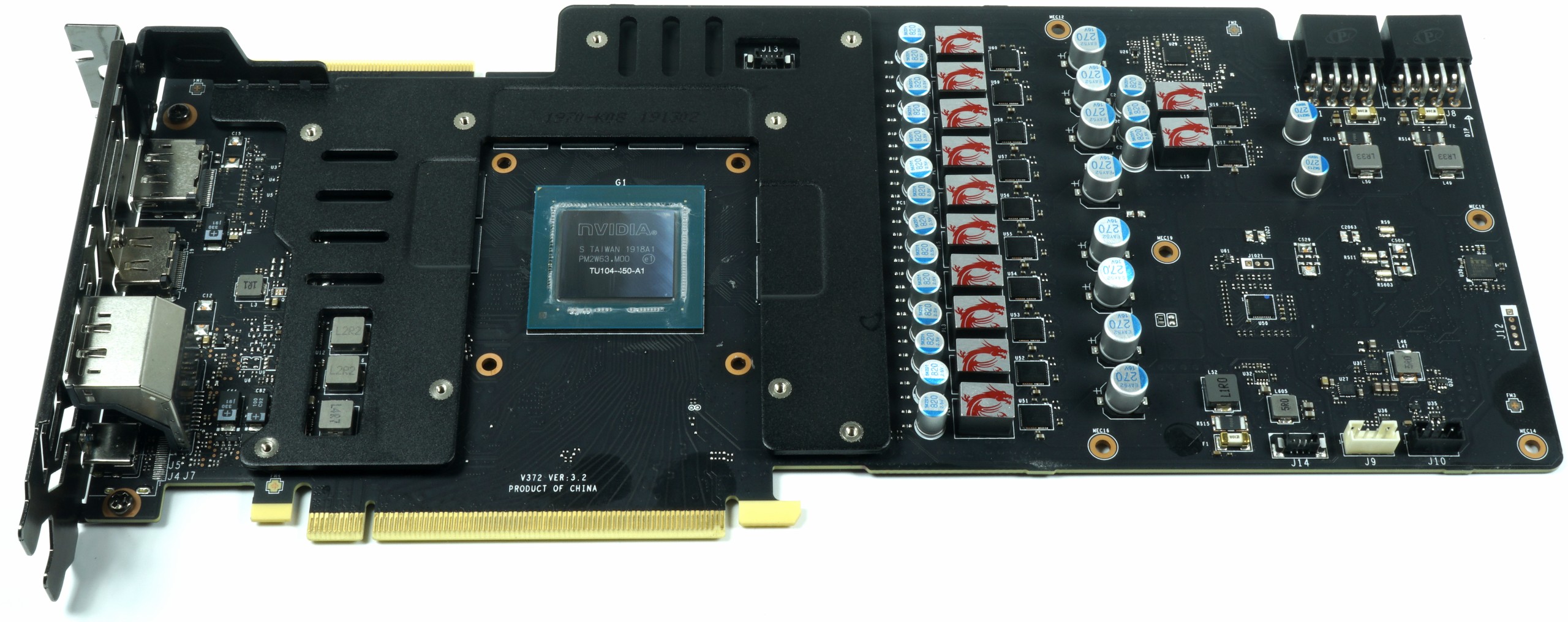
The board of the new, big sister of the GeForce RTX 2080 resembles the board of the MSI copy template almost like one egg to another. It is a rather rare design with real 10 (GPU) + 2 (memory) phases and it is convincingly solved. A total of eight phases are fed from the two external 8-pin PCIe ports, two from the motherboard slot. It also remains the same that the PWM controller for memory and the one for the GPU are both on top. The positioning of the two phases for memory can be seen by the offset to the right, while the 10 GPU phases are arranged among each other
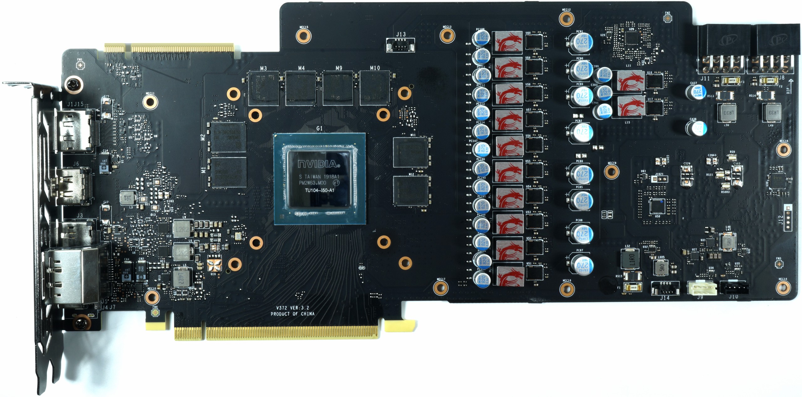
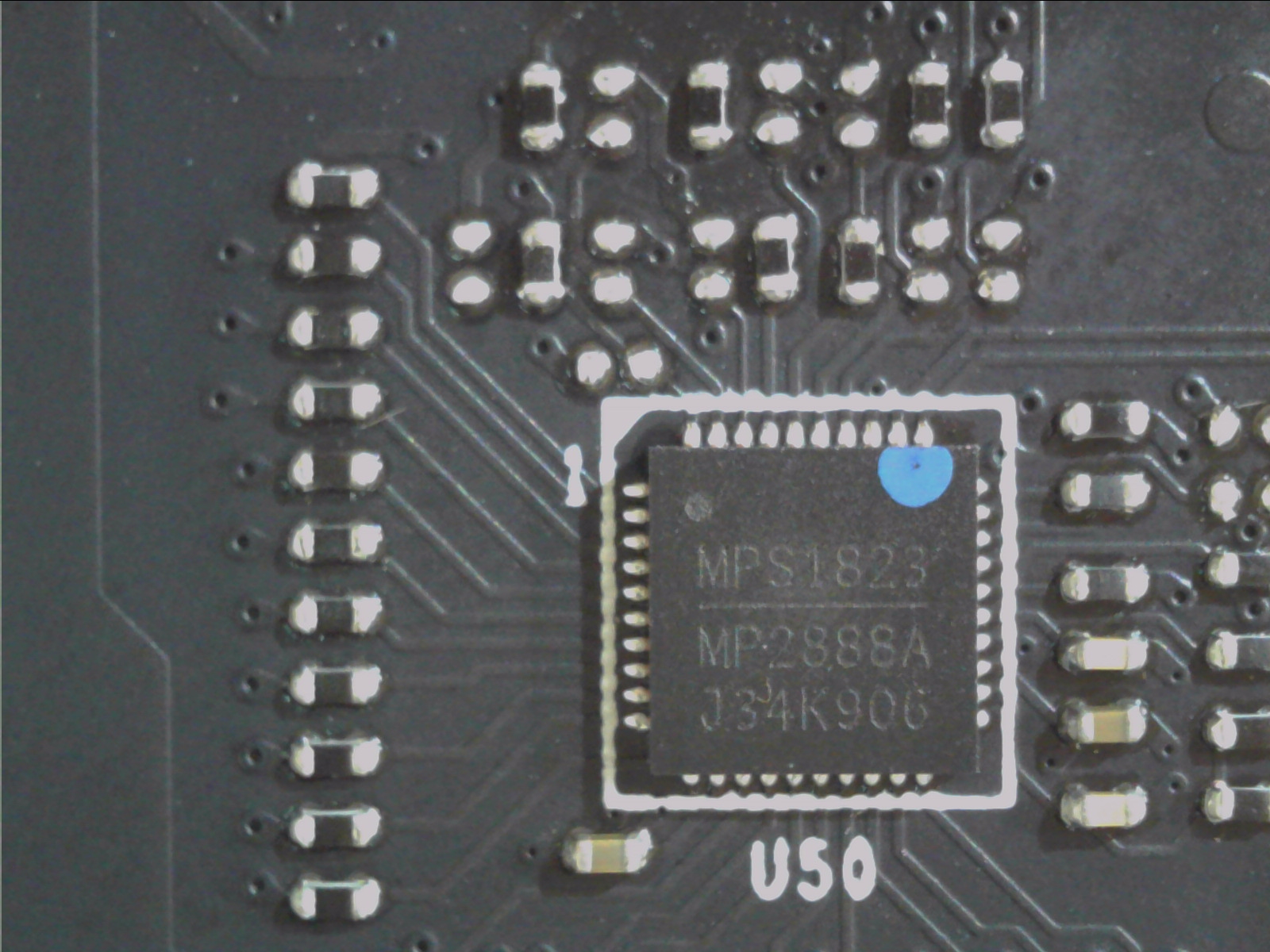
You can clearly see that the socket of the GPU is much smaller than the TU102. The MP2888A Monolithic Power Systems is a 10-phase PWM controller specifically designed to provide high-precision output voltage systems for the latest generation OF GPUs. It has programmable output voltage and active voltage positioning functions to adjust the output voltage depending on the load current, so that it is optimally positioned for a good load current transition. And it is one of the first PWM controllers that can generate real 10 phases.
The chip supports NVIDIA Open Voltage Regulator Type 4i+ with PWMVID function. The PWMVID input is buffered and filtered to create a very accurate reference voltage. The output voltage is then precisely controlled on the reference input. The integrated SMBus interface offers enough flexibility to optimize performance and efficiency and also to connect the appropriate software. The controller also supports new Smart Power Stage chips (PLCs). Appropriate PLC then provide very accurate information about e.g. currents (IMON) and temperatures (TMON).
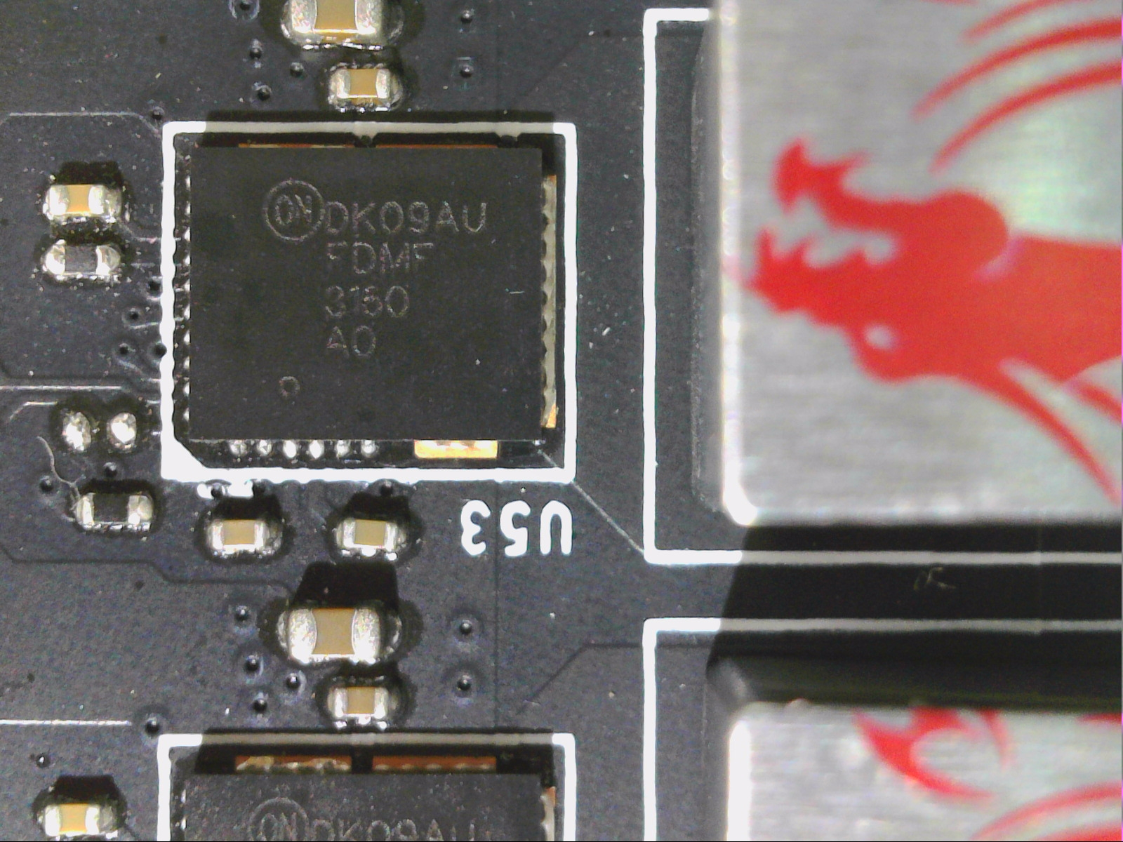
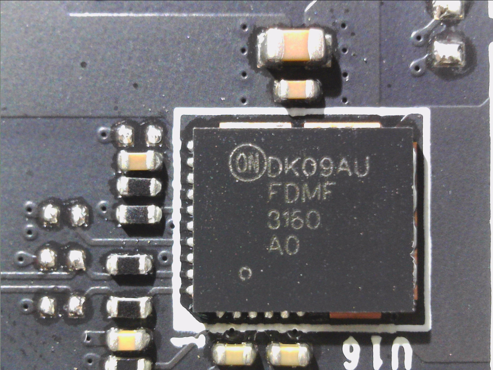
An important feature is the flexible hardware specification to adjust the operating phase number in different load current states. In addition, soft start to avoid peaks, channel current limitation, undervoltage protection, overvoltage protection and power good output. All 10 voltage converter circuits are equipped with the FDMF 3160 from ON Semiconductor, a PowerTrench® MOSFET and equivalent to the original Fairchild, which is significantly cheaper (but far from cheap).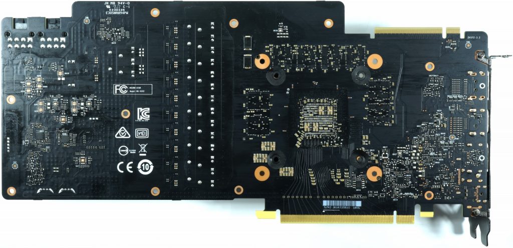
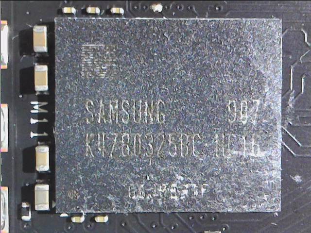
In the case of the coils, the usual encapsulated ferrite core coils, which are rectangular, are used to create more space for the high number of voltage converter circuits with the narrower sides in the vertical row of coils and to use the MSI kite labelled. The label on the memory identifies it as Samsung's K4Z80325BC-HC16. These are 8GB GDDR6 SGRAM modules with a bandwidth of 16 Gb/s. Since a total of eight modules are installed, the memory expansion of 8 GB is also available.
The two phases of the voltage converters are provided by a separate uP9512P in a two-phase layout. The two FDMF 3160s also use the same PLCs as the GPU. The coils are slightly larger at 470 mH in the inductance, but are completely identical in terms of external dimensions.
The input filtering is carried out via three 330 mH coils, whereby there is a suitable shunt in each of the three connection lines. This is a very low-impedance resistance to which the voltage drop is measured in parallel and passed on to telemetry. Thus, the board power can be limited quite exactly to what the manufacturer as a frame for the total power consumption or specified the respective supply line. The Silver Pencil faction will surely shrug nervously.
The following table contains the most important components:
GPU Power Supply |
||
|---|---|---|
| PWM Controller | MP2888A Monolithic Power Systems 10-phase PWM controller |
 |
| Gate Driver | no external | |
| Vrm | 10x FDMF3160 ON Semiconductor Smart Power Stage |
 |
| Coils | Encapsulated Ferrite Choke 220 mH |
 |
Memory and power supply |
||
| Modules | K4Z80325BC-HC16 Samsung 8x 8GB GDDR6 SGRAM Modules 16Gb/s |
 |
| PWM Controller | uP9512P UPI Semiconductor 2-phase used |
 |
| Vrm | 2x FDMF3160 ON Semiconductor Smart Power Stage |
 |
| Coils | Encapsulated Ferrite Choke 470 mH |
 |
Other components |
||
| Bios | 25WP080 Eeprom Bios |
 |
| Shunts | 1x Shunt per 12V rail (3x) |  |
| Processor |
ITE8295FN Embedded Processor |
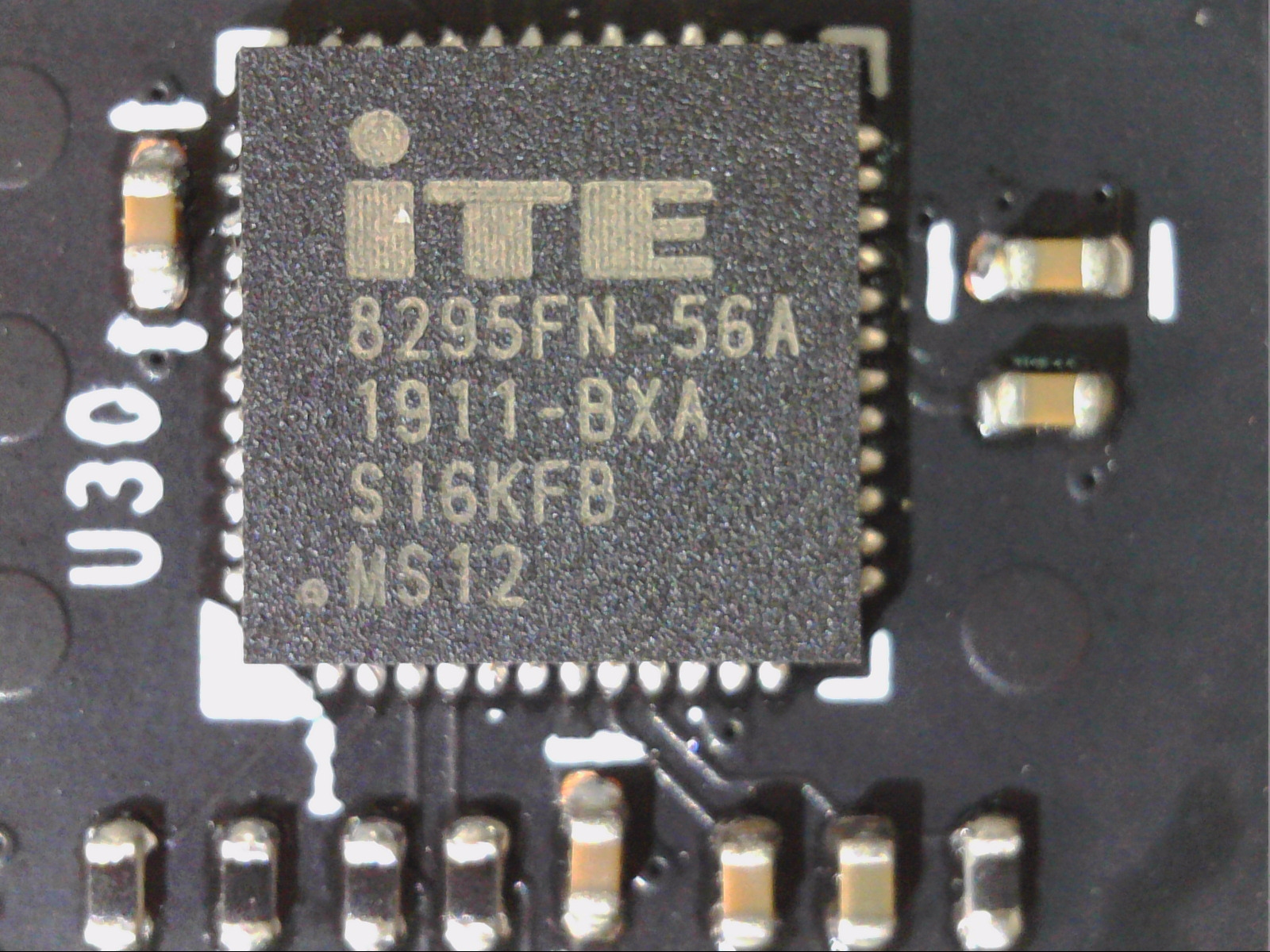 |
More details |
||
| Other Features |
8-pin + 6-pin PCI-Express connectors for power supply | |
Cooler
The top cover carries the three fan modules with each 14 rotor blades, two of which have 9.5 cm and one with a diameter of 8.5 cm. The underlying two-piece lamella cooler with the vertical cooling fins receives the waste heat from the nickel-plated heatsink via a total of six 6 mm heatpipes and a thick 8 mm heatpipe. Of the nickel-plated heatpipes made of copper composite material, two are still bent outwards in the GPU heatsink.
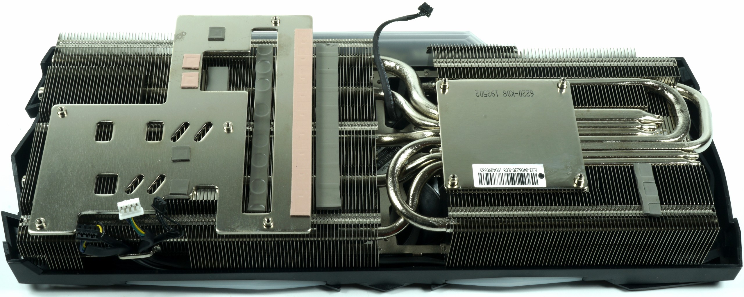
The memory modules cool MSI again via the well-known cooling frame, which is screwed to the backplate and slot bezel. And if you look closely, it's exactly the same cooler used on the MSI RTX 2080 Ti Gaming X Trio!
For the thermal transition, MSI uses three thermal conductive pads, which could have been a bit larger, even if the GDDR6 does not occupy the entire surface in the package. The pressure could have been distributed a little better, even if it is far from critical.
.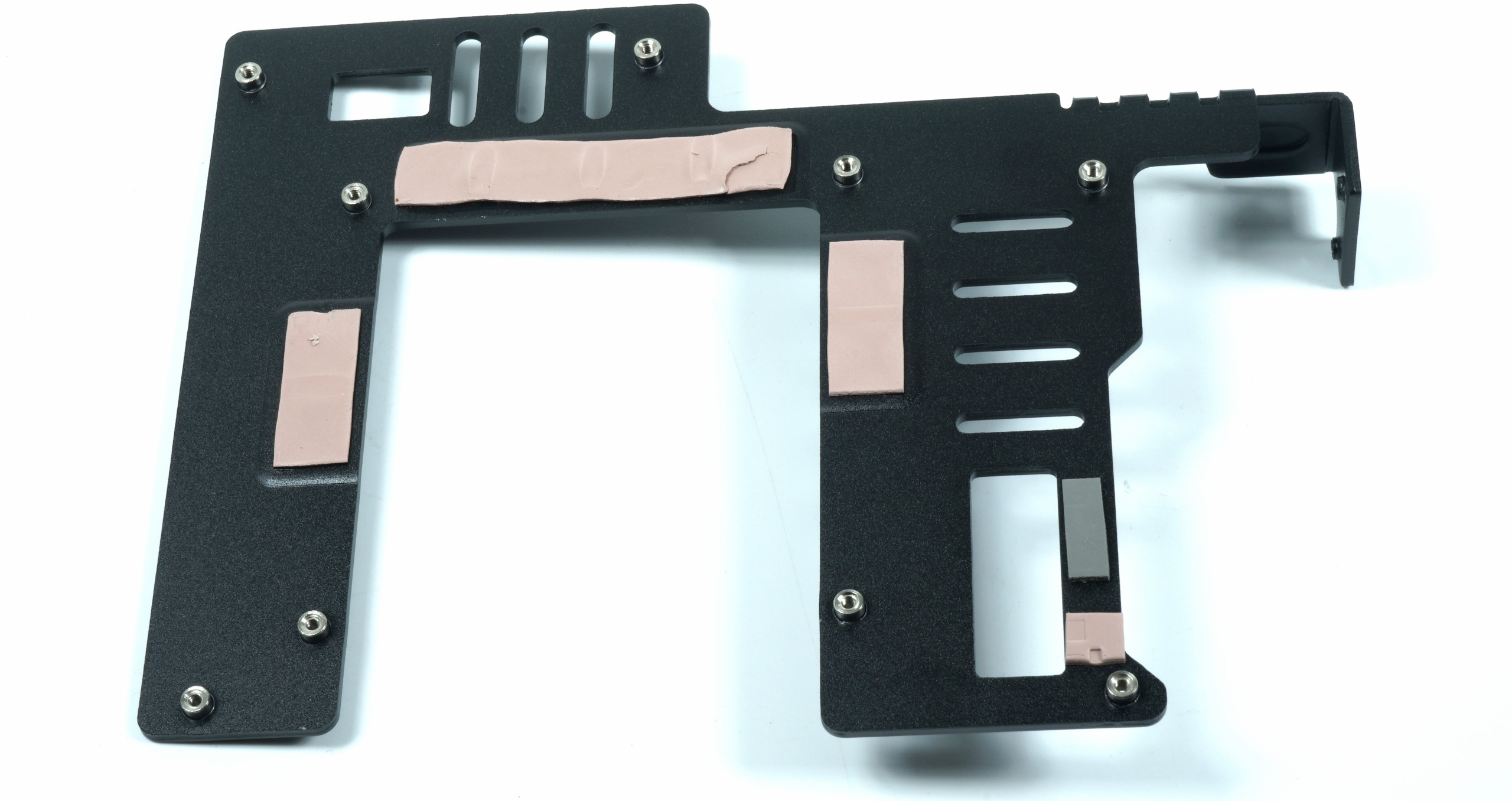
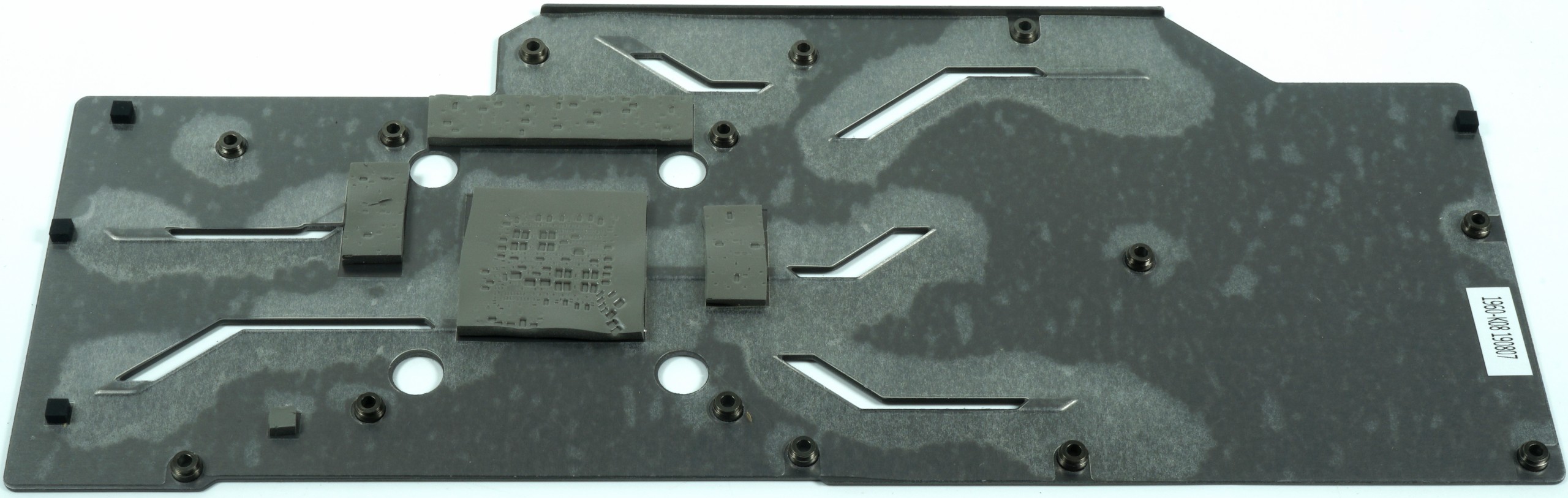
The side on the board does not save on pads and so the underside of the BGA and the memory are connected, but the voltage converters are thankfully not. The baking plate absorbs the waste heat well and is therefore much stronger and smarter integrated in terms of cooling technology than with many other cards.
| Cooling system at a glance | |
|---|---|
| Type of cooler: | Air |
| Heatsink: | Copper, nickel-plated |
| Cooling fins: | Aluminum, vertical alignment related |
| Heatpipes | 6x 6mm heatpipes, 1x 8mm heatpipe |
| VRM cooling: | About the main cooler |
| RAM cooling | About mounting frame |
| Fan: | 2x 9.5 cm fan, 1x 9.5 cm fan Fan stop |
| Backplate | Aluminum Active cooling function |


Kommentieren