


Teardown: PCB and components
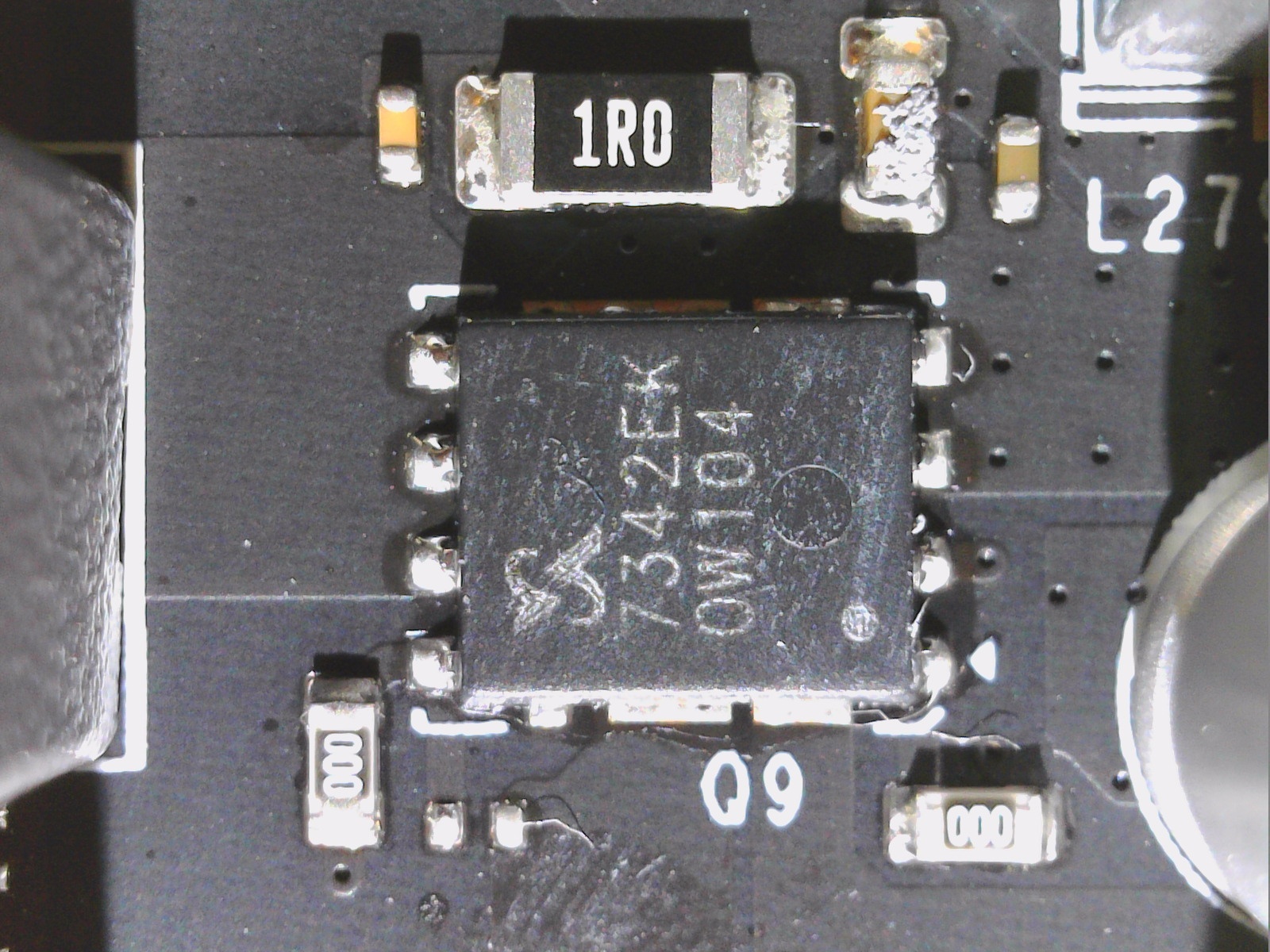
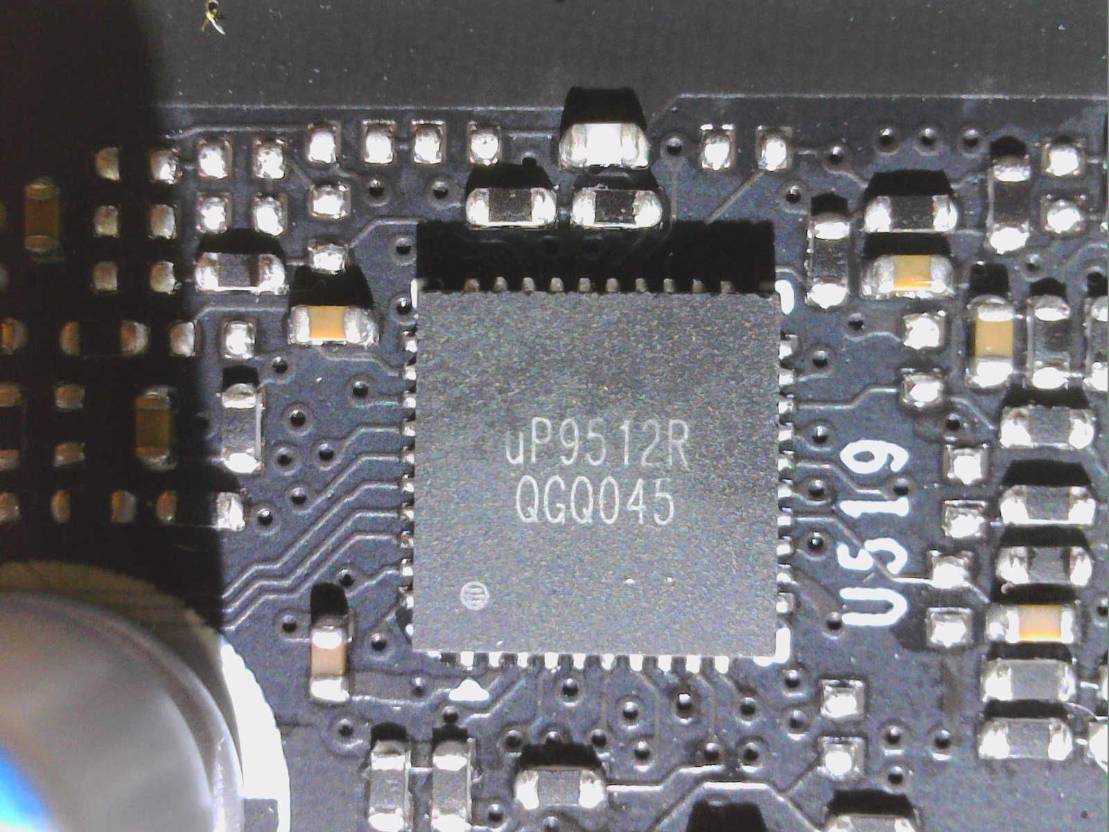
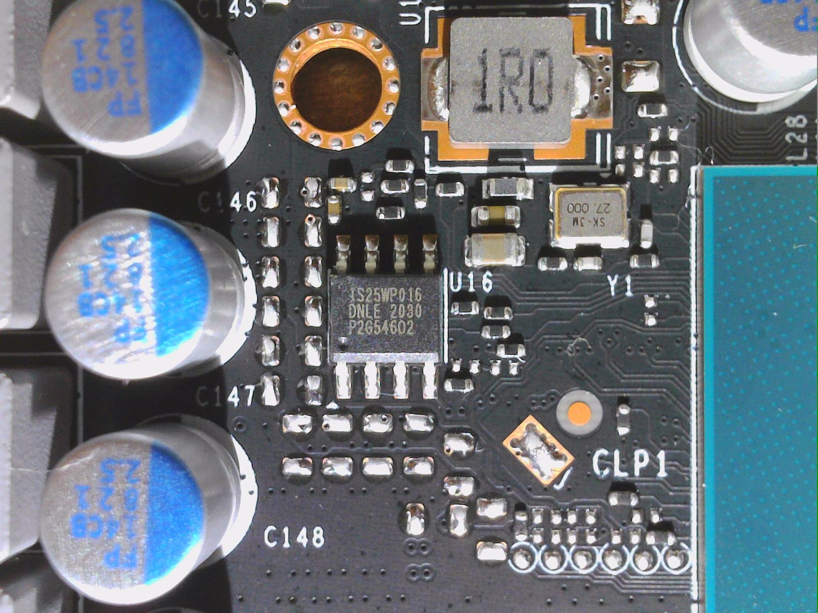
The board has been relatively cleverly rearranged. KFA2 uses a total of 8 phases for the GPU (NVDD) and 2 phases for the memory (FBVDDQ). For the 8 phases, the uP9512R is used, which is in fact the usual all-purpose weapon on NVIDIA cards. Each of the individual phases is controlled by simple SiC653A DrMOS from Vishay, which can handle a maximum of 50A. High- and Low-Side, as well as the Gate-Driver are already united in a common package and de facto result in a simple Power Stage. Vishay calls this Integrated DrMOS. However, for monitoring currents and temperatures on these simple models, one must again resort to the somewhat less accurate Inductor DCR.
KFA2 has combined all 8 phases for NVDD spatially between GPU and slot bezel among themselves. We’ll see why that makes sense in a moment with the cooler. To the right of the GPU and memory are the two phases for FBVDDQ. Here, KFA2 relies on true Smart Power Stages (SPS), in this case the AOZ5311NQI from Alpha & Omega. Again, the maximum current is 50A, but these PLCs are slightly more efficient and also provide Imon and Tmon as return values of the MOSFET DCR.
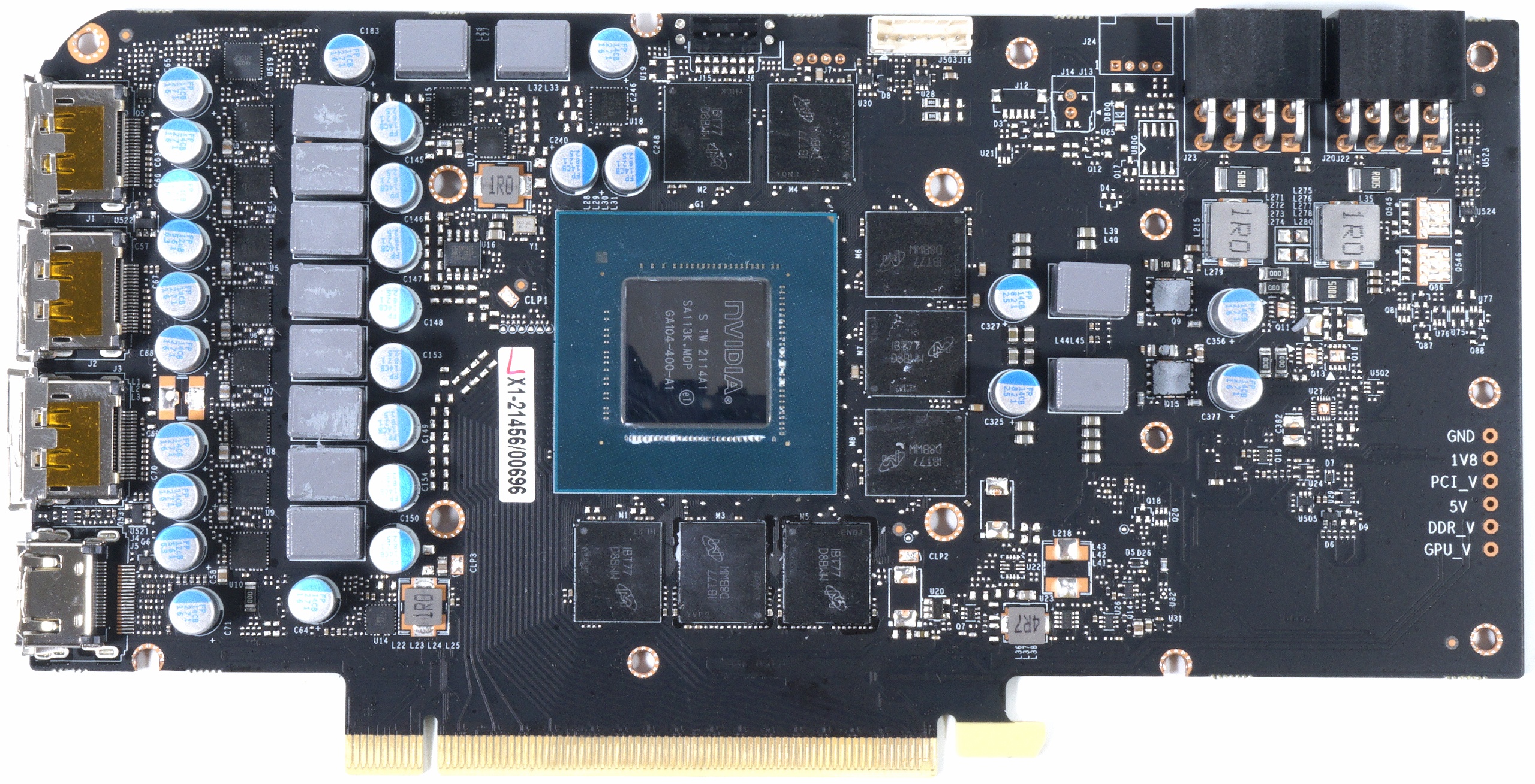
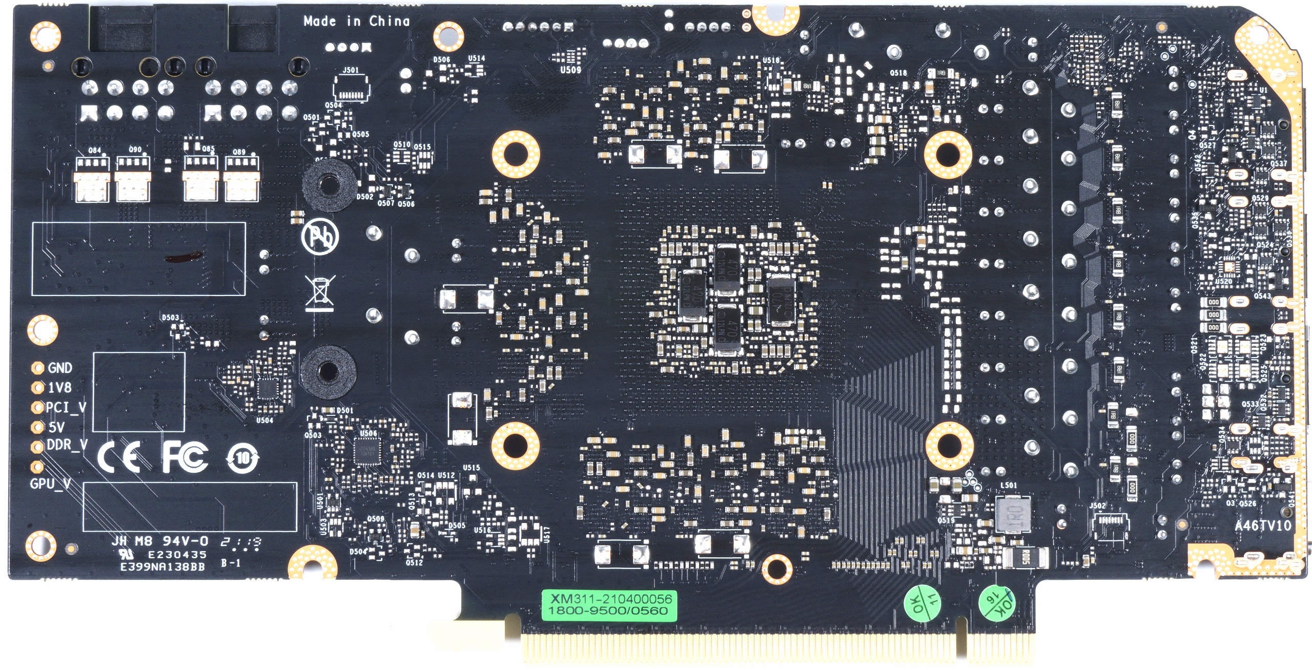
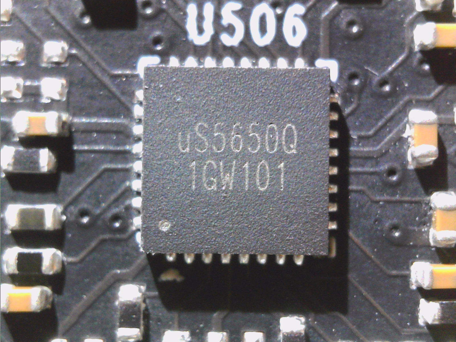
In addition, the 5 volts and 1.8 volts, as well as 0.95 volts (PEXVDD), are each generated by means of simple, single-phase back converters. This configuration is also appropriate. A normal single BIOS was installed and we also see the usual longitudinal chokes and shunts for NVIDIA’s power monitoring in the 12 volt lines, which was implemented with the usual uS5650 from UPI. The lacquered and unfortunately unlabeled coils left a decent impression acoustically, I can spoil that in advance, even though KFA2 usually uses other products. The back of the board is rather empty.
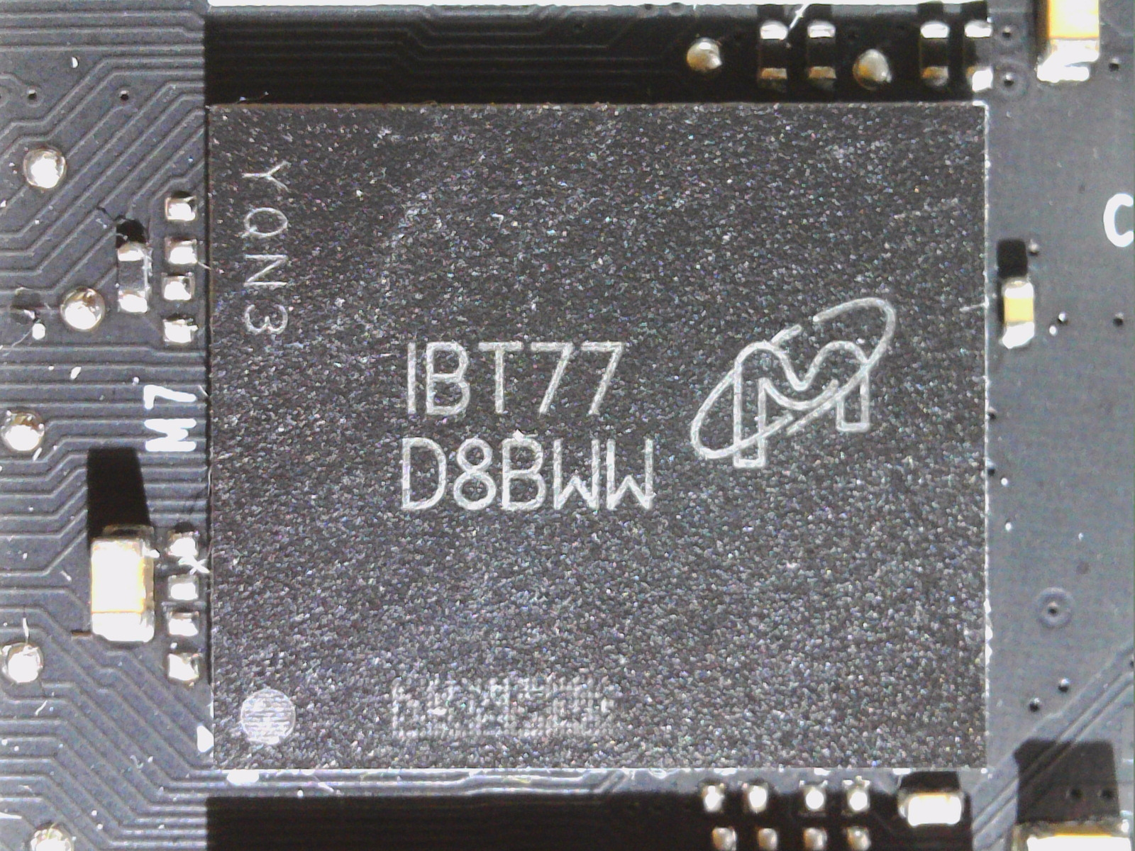
I’ve also summarized the individual components once again in the gallery below, which also shows Micron’s GDDR6X memory:

Teardown: cooler and backplate
Underneath the three 8.5 cm rotor blades (9 cm aperture) lies a rather large and clearly towering over the short PCB lammel cooler, which relies on a large, nickel-plated heatsink for the GPU and memory. The waste heat is dissipated via a total of 5 longitudinal 6 mm heat pipes also made of nickel-plated copper composite material. The three central heatpipes also lead towards the slot bracket and end directly under the heatsink for the voltage converters. Now we know why they were ordered that way.
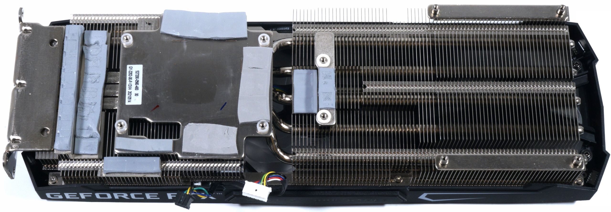
The stability of the medium-weight cooler is also due to the backplate, which is screwed to the rear, but does not have any cooling function by means of any pads. However, the cooler cools quite confidently even without this passive help. I can already spoil that here.


- 1 - Introduction and Technical Details
- 2 - Test System and Methods
- 3 - Teardown: PCB and Cooler
- 4 - Gaming Performance
- 5 - Efficiency and Power Draw in Gaming
- 6 - Power Consumption and PCI SIG Standrad
- 7 - Transients and PSU Recommendation
- 8 - Clock Rate and Temperatures
- 9 - Fan Speed and Noise (Audio samples included)
- 10 - Summary and Conclusion


14 Antworten
Kommentar
Lade neue Kommentare
Mitglied
1
Mitglied
Veteran
Mitglied
Veteran
Urgestein
Urgestein
1
Neuling
Urgestein
Neuling
Urgestein
Neuling
Alle Kommentare lesen unter igor´sLAB Community →