


From the data center to the gambler PC: Vega 20
Actually, it is with the Vega 20 as with the Titan V. Take a chip developed for data centers, scrap some features and delight the high-price community. Equal rights for all, AMD will have thought when they wanted to make Vega 20 accessible to the players. Under the hood, the AMD graphics processor Vega 20 looks very similar to the Vega 10 of the Radeon RX Vega 64. But it is precisely the shift from 14nm manufacturing at GlobalFoundries to TSMC's 7nm process that enables AMD to operate the Vega 20 at much higher clock speeds.
With its 331 mm2, such a Vega 20 is also much smaller than the Vega 10 with its 495 mm2. In the end, this also created the space needed to add two more HBM2 stacks. At the same time, the Vega 20 now has 13.2 billion transistors (compared to the Vega 10 with 12.5 billion). AMD explained that the additional 700 million transistors are used to optimize for higher clock speeds, improve hardware-based video encoding for 4K/60 Hz, and increase computing power.
We suspect that the enhancements to the compute engine referred to by AMD are more likely to affect FP64 at half-rate and support for new INT8 and INT4 statements, while the Radeon Instinct MI50 and MI60 cards, which are based on the same processor, all affect their functions, the double-precision throughput of the Radeon VII is artificially limited. Originally, AMD communicated the same 1/16 rate as the Radeon RX Vega, but this is wrong.
In reality, the double precision throughput of the Radeon VII is artificially limited to only a quarter of the single precision rate of the Radeon VII. This is much better than was initially reported. After we presented AMD with our internal benchmark data, the manufacturer revised the specifications of the card again. The VBIOS and the drivers were already designed for the higher 1/4 FP32 rate. As a result, the Radeon VII offers higher FP64 peak performance than any other AMD consumer card and is actually only behind Nvidia's significantly more expensive Titan V.
The PCI-Express 4.0 component of the Radeon Instinct MI50 and MI60 is eliminated, as are the Infinity Fabric links of the Instinct cards. According to AMD, Radeon VII's computing capabilities are designed as follows:
| Radeon RX Vega 64 | Radeon VII | Radeon Instinct MI60 | |
| Peak FP64 | 0.84 TFLOPS | 0.88 TFLOPS | 7.4 TFLOPS |
| Peak FP32 | 12.7 TFLOPS | 14.1 TFLOPS | 14.7 TFLOPS |
| Peak FP16 | 25.3 TFLOPS | 28.1 TFLOPS | 29.5 TFLOPS |
| Peak INT8 | 53.4 TOPS | 56.3 TOPS | 59 TOPS |
| Peak INT4 | 106.8 TOPS | 112.5 TOPS | 112.5 TOPS |
With the latest version of SiSoftware Sandra, for example, we were able to generate data that shows how a Radeon VII delivers incredible FP64 performance and anomalous FP16 results. But after evaluating these results with AMD and Sandra's developers, we're pretty sure they're not representative of the expected theoretical throughput of the map. AMD's official response also suggests that drivers and workloads still need to be significantly adjusted:
"Although what we shared are theoretical calculations, our initial exploration shows some compute benchmarks that are memory size and memory bandwidth intensive, where an FP64 workload on Radeon VII will perform considerably better. With FP16, we are exploring this anomaly further. However, initial exploration suggests that for this particular GPGPU workload, driver optimization will be required."
Officially, there is no really authentic block diagram, but you can take Vega 10 as a template. That's why we wouldn't really call the changes GCN 5.1, because they're actually only marginal and don't represent a real iteration.
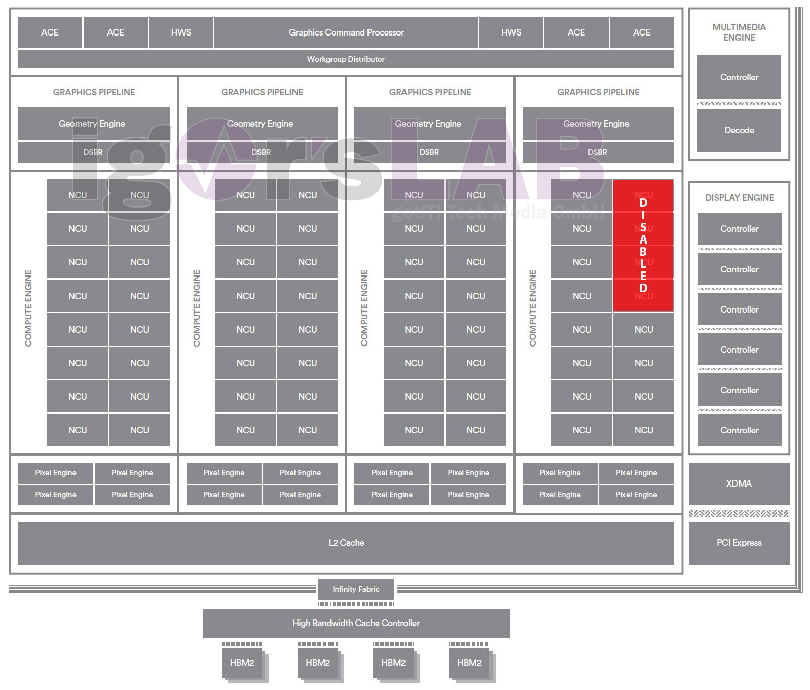
Otherwise, such a similar layout means that a complete Vega-20 chip is also equipped with four shader engines, each with its own geometry processor and rasterizer. There are also 16 compute unit (CU) per shader engine with 64 stream processors and four texture units per CU. In total, that's 4,096 stream processors and 256 texture units across the ENTIRE GPU.
But the tested Radeon VII unfortunately does not use a complete Vega 20, as it is installed on the Radeon Instinct MI60. Instead, AMD (by hardware strap?) disables four of the CUs of this chip, which results in exactly the 3,840 stream processors and 240 texture units that we also got called by AMD. You compensate for the slimming compared to the Radeon RX Vega64 by operating the Radeon VII with much higher clock rates.
The basic clock of the Radeon RX Vega64 from only 1,274 MHz increases to 1,400 MHz on the Radeon VII, while the boost clock of the Vega 64 increases from 1,546 MHz to 1,750 MHz for the Radeon VII. AMD also writes over 1,800 MHz peak clock for lower workloads, but we have never been able to achieve them in a logable manner, even with light CAD workloads.
Each of the Shader Engines of a Vega 20 also has four render backends with a capacity of 16 pixels per clock cycle and 64 ROPs. As we already know, these render backends become clients of the L2 cache. This L2 cache is 4 MB in size, similar to the Vega 10, and twice the size of the 2 MB L2 cache of the Fiji chips. Although a large L2 cache helps keep frequently used data close to the GPU, Vega 20 shouldn't be as dependent on Vega 10's, thanks to a more balanced storage subsystem.
The Radeon VII also extends the RX Vega's memory expansion to four HBM2 stacks, resulting in an aggregated 4,096-bit path at the end (the Fury X sends greetings). But a data rate of 2 Gb/s allows us the amazing bandwidth of 1 TB/s, which should be a certain advantage not only on paper.
The multiple BIOS of the Radeon RX Vega with several power profiles is no longer required by the Radeon VII. The indication of the 300 watts of TBP is real, even if you could of course push this value significantly by doing it manually – if you wanted to. On paper, by the way, that's 5 watts more than the maximum for an RX Vega 64 at the time. However, it is pointless to make any considerations of efficiency at this point, because we have not yet set anything.
Thermal monitoring
What is fed to the card must also be dissipated at the end almost 1:1 as waste heat. This is exactly where the cooler and the selected fan profiles come into play, which I want to spoil at this point for a short time, have led to an awkward frown. But I will come to this later, because for every claim I also have very detailed measurements with professional equipment at hand. First, though, I'll discuss what AMD has reintroduced.
Specifically, it's about trying to get more power out of the GPU through improved thermal monitoring. Instead of measuring temperatures with 32 sensors inside and outside the GPU, as was the case with the Vega 10, the Arbitrator now obtains data from 64 sensors strategically placed in and around the Vega-20 chip.
And while the barrier layer temperature (Tjunction), which was derived from these sensors, at that time only controlled the thermal shut-off protection, it is now also used for throttling and fan control. Which would also confirm my investigation into the ominous "hotspot" at the time. Even if a monitoring software, for example, only a GPU temperature of 75°C or 80°C, the actual peak temperature in some areas of the barrier layer can already be 95°C or more. But then the fans are turned up to almost 3000 rpm.
The bottom line of all this is that AMD now wants to be able to be more aggressive when it comes to keeping Vega 20 at high clock speeds, simply because there is more data from a larger network of sensors, and then know with reasonable certainty that other areas of the graphics processor are not at temperatures outside of safe limits. You get higher FPS rates, but in return you can also be "punished" with higher fan speeds.
This time I also included a video from my audio chamber and recorded the fan noises recorded by the measuring microphone. In addition to a documented analysis of the frequency spectrum, it will thus become a certain unique selling point of this review. Another highlight, by the way, is the board analysis. Please keep a leaf ingession…
- 1 - Einführung und Daten
- 2 - Vega20 - Was ist neu?
- 3 - Tear Down: Platinen-Analyse und Kühlerdesign
- 4 - Anwendungsbenchmarks
- 5 - Ashes of the Singularity: Escalation
- 6 - Battlefield V
- 7 - Destiny 2
- 8 - Tom Clancy's The Division
- 9 - Far Cry 5
- 10 - Tom Clancy's Ghost Recon
- 11 - Grand Theft Auto V
- 12 - Metro Last Light (Redux)
- 13 - Rise of the Tomb Raider
- 14 - The Witcher 3
- 15 - Wolfenstein II: The New Colossus
- 16 - Leistungsaufnahme und Netzteilkalkulation im Detail
- 17 - Temperaturen und Infrarot-Analyse
- 18 - Lautstärkemessungen mit Video und Analyse des Spektrums
- 19 - Zusammenfassung und Fazit


Kommentieren