NVIDIA does everything right, actually…
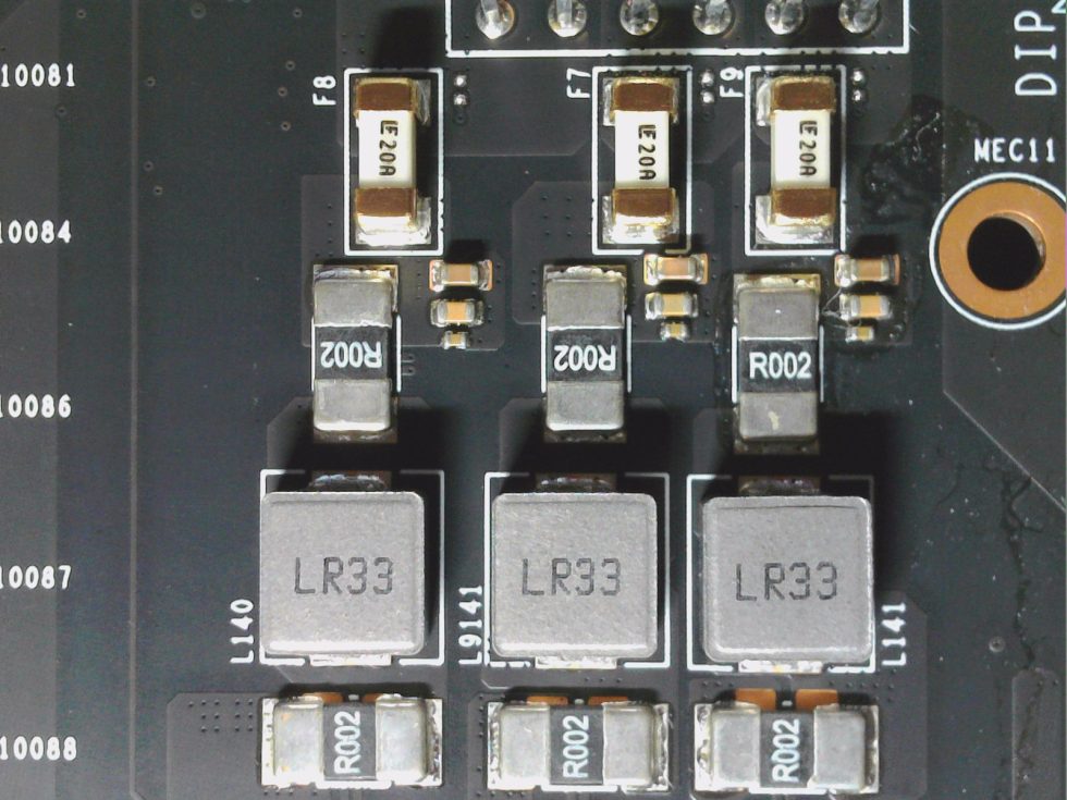
NVIDIA’s monitoring is done on the board at the respective 12-volt rails, i.e. at the respective external PCIe sockets (Aux) and the motherboard slot (PEG) BEFORE the respective consumers are supplied. This task is done, similar to my already shown measurement setup, with so-called shunts in the input area just before the filtering directly at the respective rails. The very low impedance longitudinal resistors (shunts) used produce a small voltage drop, which is made possible by two voltage taps (before and after the resistor). The approx. 1.5 to 5 watts (depending on the flowing currents) that occur here do not yet fall into the TBP budget (power limit) of the graphics card.
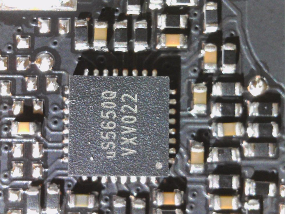
The whole thing is then calculated with a suitable monitoring chip, which can usually monitor up to four channels. The voltage difference can be used to infer the flowing current and, together with the output voltage downstream of the shunt, even the power consumption in watts (W). So the whole thing is basically nothing else than my already shown measurement setup and thus also valid for the TOTAL card!
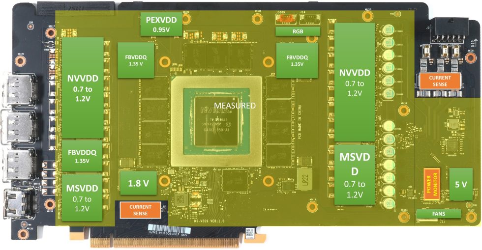
Now let’s look at the graphics card as a scheme. We see here as “Current Sense” the two places where the currents (and voltages) are sensed and where then in the “Power Monitor” the data is generated for the firmware to meet the power budget. We can see in the yellow highlighted area that both the GPU and the memory and all other consumers including their voltage converters (and their losses), as well as the losses of all components and even the board are included. Thus, NVIDIA understands Total Board Power (TBP) as the power consumption of the entire graphics card including fans and RGB gadgets!
The firmware (and of course Boost) can now ensure that this maximum value is never exceeded for a longer period of time and that the default value is maintained again in a larger interval. All these values can be read out and used quite easily via the NVAPI (programmer interface). Here you can also see which maximum or minimum value is permissible or has just been set. Programs like MSI Afterburner also orient themselves on these values when it comes to the start and end values of the slider for the power target to be selected. In the worst case, the set power target is equal to the max power limit stored in the firmware and you can no longer increase anything manually.
Why performance drops sharply with hot cards
We know the effect that with fully warmed up NVIDIA cards (especially with poor cooling) the clock (and thus the performance) drops more than it is observed with mostly AMD graphics cards. This, in turn, is due to the way NVIDIA manages its very restrictive power budget. People usually blame the lack of the highest boost steps on warmed-up cards on the GPU and leakage currents, but this is only part of the truth. The smallest, mind you, because the greatest losses are incurred by the hot voltage transformers!
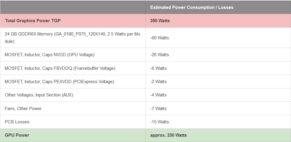
Many people are not particularly aware of the fact that voltage converters have to be cooled as well as possible. But the losses that occur here are enormous! If a normal regulation with Smart Power Stages (SPS) or DrMOS for NVVDD/MSVDD (i.e. the GPU) usually works with an efficiency of 85% and higher when the card is cold, this efficiency drops to as low as 80% if the voltage converters get hot. The more efficient and higher-quality these components are, the smaller this effect is. With a discrete low and high side consisting of single MOSFETs as well as separate gate drivers, some cards do not even reach 80% in cold state and this value can then even drop below 75%! All the power that is lost here and already converted into heat is lost to the GPU later. This also applies to all other components that generate power dissipation, no matter where they are located on the board.
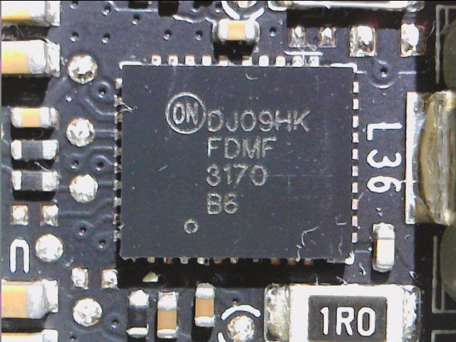
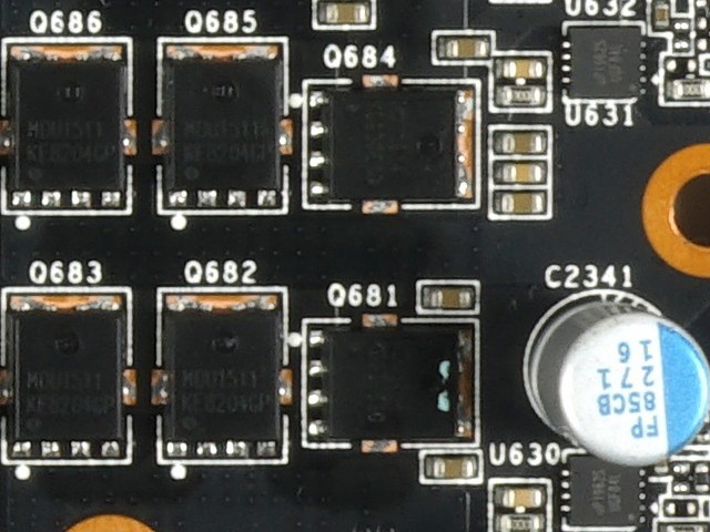
It’s no coincidence that Nvidia has moved away from the so-called phase doubling, where the up to eight real phases that such a PWM controller can provide are virtually doubled by means of so-called doubler chips by simply driving the newly generated phase out of phase. In the meantime, however, there are also PWM controllers that allow parallel and thus in-phase operation of several voltage transformer circuits. In the following picture we see on the left a highly integrated Smart Power Stage (SPS) with integrated high-side and low-side, as well as gate driver and Schottky diode. On the right, we see two discrete phases, each with a MOSFET on the high side (Q681 and Q684) and a parallel pair on the low side (Q686+Q685 and Q683+Q682), as well as an external gate driver (U630 and U631)
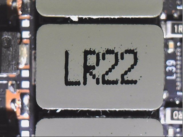
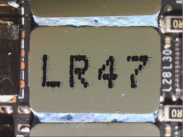
However, since capacitors alone are not sufficient to achieve a high-quality and ripple-free voltage at the end of the PWM nodes (see also the operation of a switching power supply), the output of the voltage converter circuit is terminated with an LC element (coil + capacitor). These coils, which store and then release the briefly charged energy, have both electrical and inductive resistance, which pushes efficiency down yet again. Sounds like an unsolvable problem, and by the way, it is, because you can’t endlessly increase the cross-sections of the windings to at least lower the ohmic resistance. Especially since the inductance remains. In the picture below we see a typical coil for the GPU phase on the left and one with higher inductance for the memory on the right. Although lower values are now being used again for this purpose as well.
In addition, of course, there are synchronization and balancing problems, the more phases you condense in this way. In the meantime, however, PWM controllers are capable of intelligently controlling the utilization and use of phases at low and partial loads. But how does all this affect the GPU itself? For example, a card that consumes a total of 350 watts of power (example of a GeForce RTX 3090 FE) can effectively use 230 watts of it when cold. If the efficiency of all installed voltage transformers drops sharply due to extreme heating, that’s still 200 to 210 watts that remain!
Readout via software is possible and plausible
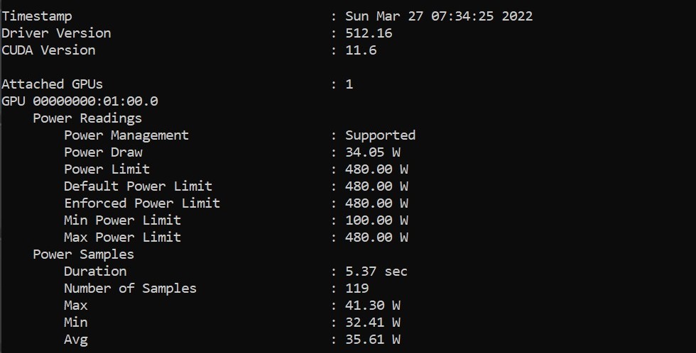
The good side of NVIDIA’s control and limitation mania is the fact that you can read the performance limitation and monitoring values quite easily and accurately via software. The very rough intervals do not allow any statements about load peaks, but if you log over a long period of time, the result is hardly different from what I can measure as a long-term value with much more elaborate technology in the same length of time. The results of the current MSI Afterburner, GPU-Z and HWInfo can therefore be trusted. more on this later.











657 Antworten
Kommentar
Lade neue Kommentare
Urgestein
1
Urgestein
Veteran
Mitglied
Veteran
Urgestein
Urgestein
Urgestein
1
Urgestein
1
Urgestein
Urgestein
Urgestein
Urgestein
Veteran
Urgestein
Urgestein
Alle Kommentare lesen unter igor´sLAB Community →