


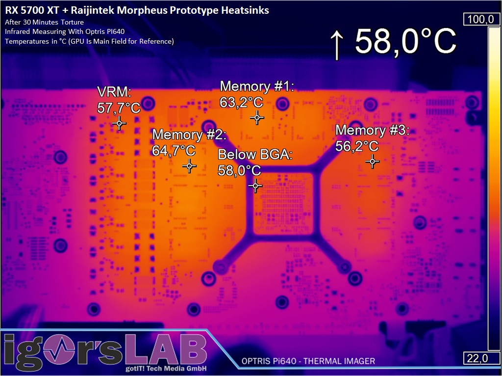
Measurement von Tboard on back side of the PCB
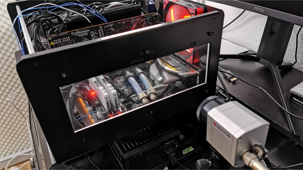
I’ve already talked about “tropicalization”, so that I’d classify the measured values as reliable. In spite of the good equipment, I would expect a tolerance of about 1 degree, but not more. Furmark is used, which I let run for 30 minutes until I measure finally. The room temperature is 22 °C, the setup is open this time, because I need a constant ambient temperature. On the PCB you can see the difference between the memory modules, which are located on the side between GPU and VRMs, and those on the top side of the PCB, which already act a bit cooler and are not negatively influenced by the interactions of the other hot areas or the copper traces.
This measurement clearly shows why it is possible to save copper for the three memory modules acting much cooler here on the right. Aluminium is also good enough at this point, but costs much less. So I was able to measure at the hottest spot on the board just 65 °C below the memory and it will be interesting to see what happens on the upper side. By the way, I also recorded the temperature curve with the software PIX Connect from Optris that fits the camera, in order to be able to include this data in the next graphic.
Measurement of Tcase on the top of the memory and of Tjunction in the memory
Now the logger, which records the type K sensors at 1-s intervals, and the GPU-Z are also used. I use for the curves, because AMD considers only the hottest module, the highest of the values measured for Tcase and the corresponding data of the measurement of Tboard with the infrared camera. The result is not surprising when you know how the individual temperature resistances of the layers turn out, but the normal user will now be quite amazed.
I also have to correct myself a bit, as the values for Tjunction seem quite plausible on closer inspection, considering the high thermal density due to the rather tiny chip inside the large package. But before I draw my final conclusions, let’s have a closer look at the curve of all temperatures:
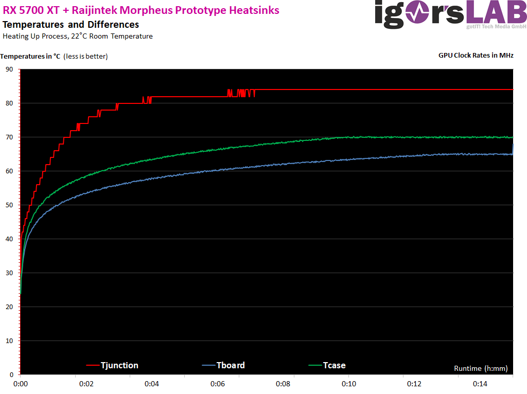
After heating up, everything remains constant from minute 13, so you can always assume the final temperature, which does not change even after 30 minutes. In order to be able to recognize the process better, the diagram also shows an end after the 15th minute. The inside of the GPU reports approx. 53 °C, the underside of the circuit board is considerably hotter at approx. 58 °C. And what happens to the memory modules?
The hottest one (module #2 on the IR image) is located near the voltage regulators and brings it to a Tboard of approx. 65 °C, a Tcase (including the explained offsets) of approx. 69 °C and a Tjunction inside of 84 °C. This results in a delta of 15 degrees between chip and module top and of 19 degrees to the board bottom with this very good air cooling and without backplate cooling for the memory.
Earlier experiments with a water block and many backplate vs. pads variants have shown further interesting influences. If you only cool the memory on the backside with a good pad between the backplate and the board, Tboard sinks another 4 degrees, which also lowers Tjunction by 1 to 2 degrees. The Tcase is also much lower than Tboard when it comes to water cooling, which could make rear cooling all the more interesting.
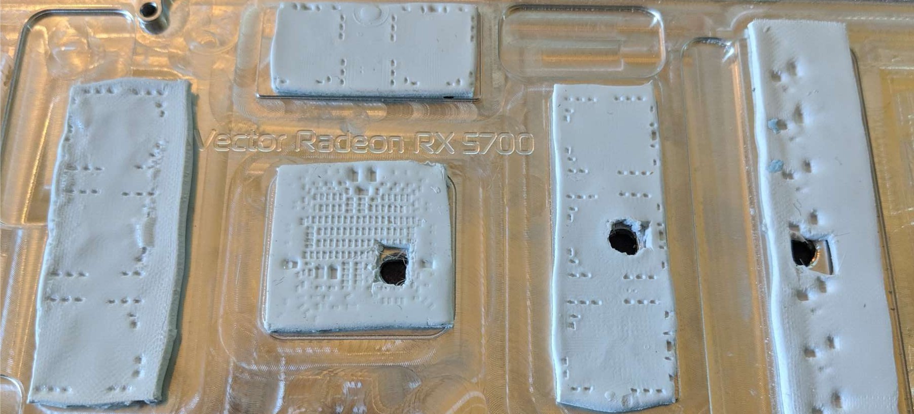
Various tests with different pad materials have also shown that a large-area coating with very good, continuous contact and the inclusion of higher components and solder points in the pad material with the help of special ultra-soft pads (see above) performs better than nominally (in terms of thermal conductivity) better pads, which, however, are more rigid and also tend to bleed the silicone. Nvidia was the first major graphics card manufacturer to rely on these pads, and rightly so.
Conclusion and bottom line
It is no secret that memory modules inside can become significantly hotter than the outer surface on the top of the module package or the underside of the circuit board would suggest. But the delta of 15 degrees to the surface of the package still seems relatively high to me. If you now use the same tjunction of 100 °C for GDDR6 as for GDDR5, with a surface temperature of approx. 85 °C, it would already be an end to fun. But even such a high value is no reason for premature panic, if one understands the relationship of all temperatures.
What does that mean for me? Since the glued heatsinks in my test are not the last end of the wisdom, but are sufficient for this test setup, a water cooling however reaches clearly lower delta values and then even the back of the board becomes warmer than the package above, I must probably add in the future with my graphics card tests a further measurement and consideration, in order to be able to conclude reliably from Tboard to Tcase. And in the end I proved to myself the opposite of what I had publicly advocated in good faith. It’s nice if you at least do it yourself, so the insight is easier. 🙂
But it’s also a fact, that the read out Tjunction could be correct, if you look at it as a pure worst case value, which explicitly captures the temperature peak inside the hottest memory module and nothing else. If you cool this down more and leave the rest unchanged, the firmware looks for the next hotspot. So you should take Tjunction very seriously, because minus all tolerance values the result often seems to be very high, but also reasonably plausible.
Unfortunately, AMD and its board partners are rather cautious when it comes to the exact use of this value for performance control (throttling down) or safety features such as shutdowns, but the effort will certainly not have been made for nothing. Whether Nvidia reads and uses similar values internally could not be reliably determined until now. With the open sensor data one finds in any case up-to-date nothing. If there is something new, you will of course be the first to know, I promise.


Kommentieren