


Are there any major changes to PCB layouts in terms of capacitor and IC locations, new JEDEC layout standards for single or dual-rank layouts?
Yes, the JEDEC committee has designed brand new PCB layouts for the introduction of DDR5. Because a Power Management Integrated Circuit, PMIC, was added to each DDR5 module, new power routing and distribution layouts were required, which was not the case with DDR4.
What about the PMICs? Will high-end Kingston kits already use an “unlocked” PMIC that can deliver more than 1.435V VDD/VDDQ?
All Kingston FURY Beast DDR5 PMICs are enabled for XMP 3.0 profiles 4 and 5 to enable programmability for users. However, to avoid damage to the CPU and the DRAM components, there are limits to the voltage level that can be set. Depending on the brands, some motherboard BIOS settings allow a wider range of voltage adjustments.
Again, this probably sounds familiar to most readers. The power supply of the memory modules with the “RAM voltage” was still done with DDR4 via voltage regulators on the mainboard, which convert 12 V or 5 V from the power supply to the typical 1.35 or 1.5 V to the DIMM slot. With DDR5, 5 V go directly via the DIMM slot to the memory module, where the PMIC is located, which generates the voltages that can be digested by the memory ICs.
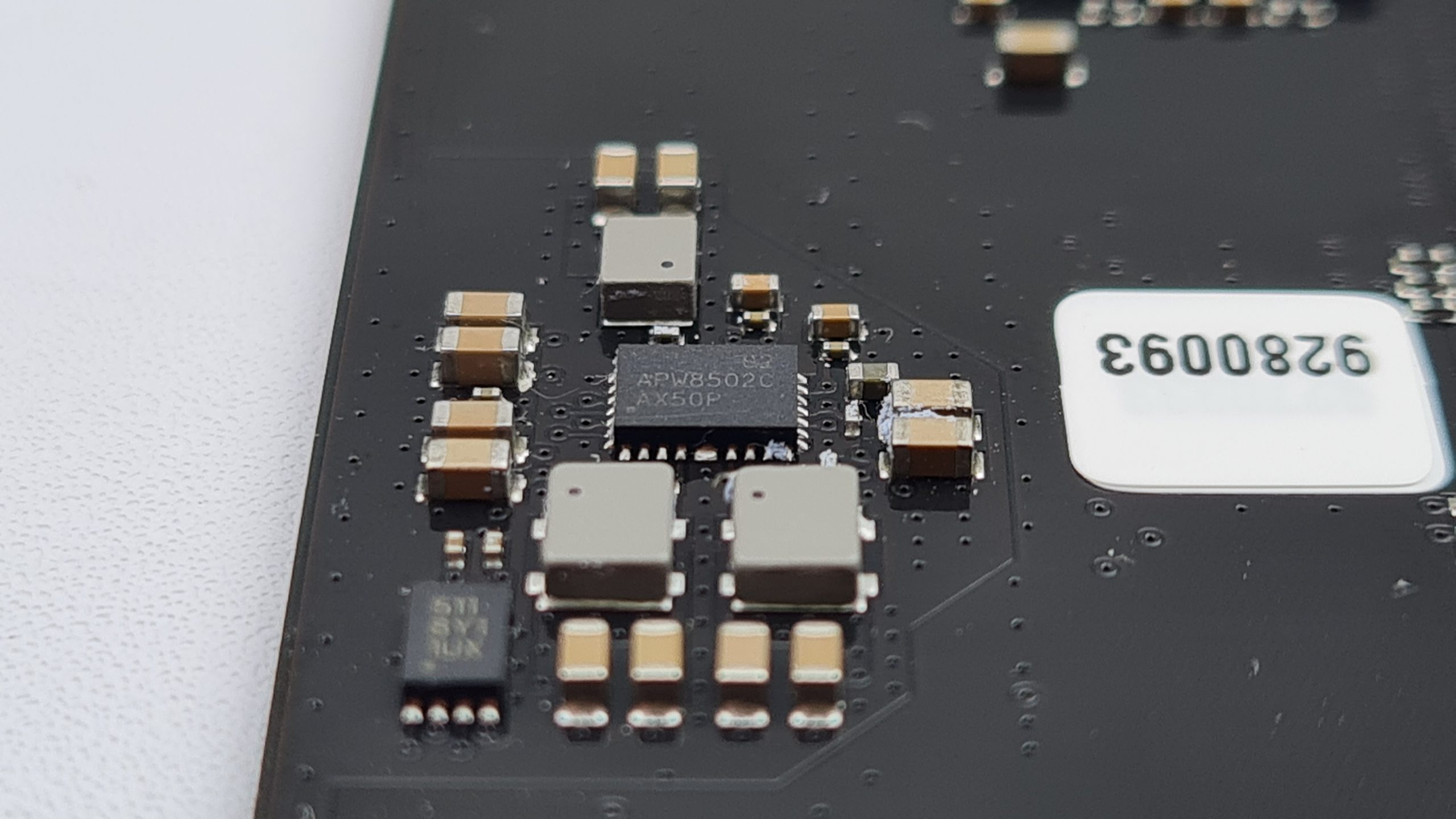
Unlike DDR4 there are now two main voltages, VDD and VDDQ, which are typically 1.1 – 1.435 V and depending on the IC also want to be set independently of each other for best possible OC – that’s just as additional info from me. For voltages beyond the 1.435 V limited in the standard, special unlocked PMICs are required, which we have not yet been seen on any freely available DDR5 module. For RAM overclockers, the module selection becomes even more complex. According to some news sources, these PMIC chips and not the actual DDR5 memory are probably the reason why the new modules are currently still so scarce. Here, many manufacturers have only recently started production, which of course explains the delays in the entire production chain.
On the subject of manufacturing, I was also immediately interested in what the new board layouts are called. Because with DDR4 one could already conclude approximately on the basis of the layout type, like e.g. A0, A2, B1 etc., how high or low a module can be potentially clocked.
Is there any information yet on what the PCB layouts are called (e.g. JEDEC A2 or B1 for DDR4)? There are now no capacitors at all on the bottom edge of DDR5 modules – what is the reason for this?
The current JEDEC standard raw cards for DDR5 UDIMMs are: A0(1Rx8), B0 (2Rx8) and C0(1Rx16). Component placement has been changed in DDR5 compared to DDR4 to allow for better data and power management and to reduce susceptibility to damage near the edges of the module. Passive components at the edge of the module were an occasional problem with DDR4: pressure during insertion occasionally damaged or detached the components. Often this could only be seen on a microscopic level.
As with DDR4 the single-rank layouts start with A and dual-rank layouts with B, where the revision is simply incremented with a number, ergo A0 or B0 – so far so logical. It is also interesting that with C0 there is a standard for 8 GB modules with x16 ICs. Also with DDR4 there were already such x16 memory chips, which were often used in notebooks or servers, where the raw performance is not as important. Simply said, here one memory chip takes over the work of two, so that already with 4 memory chips a complete module can be built.
This is where the aforementioned banks come into play again, effectively having to do twice the work, often at the expense of performance. But since there are now also twice the number of bank groups per memory chip with DDR5, the performance deficit should at least be less than with DDR4, at least on paper. And similar to DDR4, these x16 variants could again have a second pair of modules in dual-rank effectively delivering the same performance as x8 modules. Even if there are mainly only 16 GB 1Rx8 modules available at the launch of DDR5, this info could be interesting for one or the other special use case.
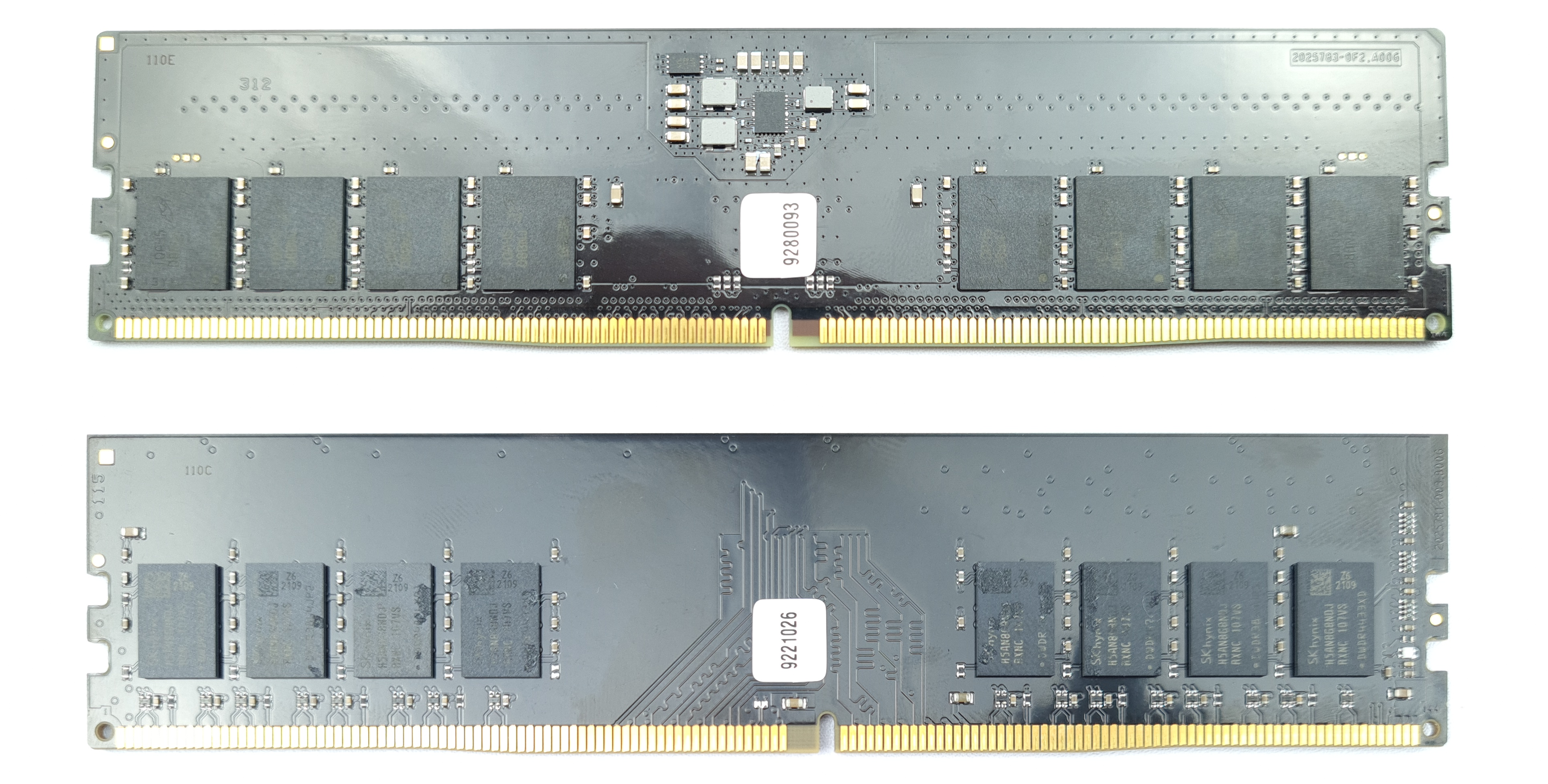
Also, the capacitors at the bottom of the modules are now completely omitted with DDR5. Anyone who has ever bought used RAM on ebay will know all too well the problem of a capacitor and its RAM module arriving separated from each other due to improper packaging. But also when inserting the modules into the DIMM slots, it is easy to get caught on something and accidentally damage a solder joint of the tiny components, which you might only notice in the end by instabilities or a worse clock rate. Thankfully, the DDR5 standard has removed these lower edge components from the boards altogether.
The DDR4-5333 module from Kingston that you can just see was only recently in our review. In order to achieve these high clock rates stably with the old standard, one had to reach deep into the production trick box and distribute the signaling over 12 board layers. The question arises whether DDR5 with similarly high speeds even with entry-level SKUs is already significantly more expensive to manufacture here.
What are the changes from DDR4 to DDR5 (e.g. PCB Layer Count)?
As a memory module manufacturer, the transition from DDR4 to DDR5 involves additional components such as PMIC, inductors and more. However, because our SMT assembly lines can manufacture a variety of products simultaneously, including SSDs and USB flash drives, this next step in DRAM module production is not a problem.
Kingston DDR4-5333 is already on 12 layers. How many layers do the first DDR5 kits have?
PCB layers are determined by the JEDEC committee through the Raw Card Design and may vary depending on the number of ranks and DRAM types supported. DDR5 modules have between 8 and 12 layers depending on the type. In some cases, PCBs for overclocking deviate from the JEDEC standard raw cards to enable higher performance. These are compatible, but are not considered standard.
The “slower” DDR5 kits therefore still manage with 8 layers, which could also have a positive effect on the manufacturing costs in the long term. I was also able to confirm the Fury Beast DDR5-5200 kit that Kingston has already provided us with as an 8 layer board. Conversely, there is still a lot of room for improvement on the manufacturing technology side, in order to be able to offer even faster modules in the future.
Especially interesting for us enthusiasts and overclockers are of course the memory ICs installed on a module. In the DDR4 era, Samsung’s 8 Gbit B-Die had emerged as the absolute performance leader. For example, the Fury Beast DDR5 modules use Micron 16 Gbit Rev A memory chips, which hit a clock speed limit of around 5600 Mbps in our tests. So if there are already DDR5 modules with XMP profiles of 6000 Mbps and more, they must be different memory ICs, right?
Currently only the DDR5 manufacturers Samsung, Micron and Hynix have leaked, but no specific IC type names. Can they be named already, DDR5 ICs are available in general – independant from the usage in Kingston products or their overclocking capabilities?
We understand “overclockers” who want to know which are the best ICs by brand and revision. However, since we have been manufacturing memory modules for overclocking for almost 20 years, we can safely say that DRAM brand and revision are not always consistent. We source from all three major DRAM semiconductor manufacturers. And when we set specifications, we usually do so with multiple DRAM options. A single DRAM chip as the source of a given speed, latency and capacity is not viable for a global customer base.
Moreover, a single DRAM die revision can lead to significantly different results in a single production batch during the screening process. The only way to guarantee higher DRAM performance is to select DIMMs or kit part numbers that are factory preset for high speed.
We expect there will be some winners and losers in overclocking DDR5 DRAM over time. Apart from this, improvements are constantly being made by DRAM semiconductor manufacturers to increase yield and quality, which translates into higher performance in internal screening. A DRAM revision today that has low overclockability may see dramatic improvements in the coming months as the vendor refines the production process.
Of course Kingston is right, because on the one hand there are, as always in the silicon lottery, better and worse bins of each memory IC and on the other hand the board design and the production quality around it must also be right. To be fair, it has to be said that Kingston’s fastest DDR5 modules with DDR5-5200 are not yet among the absolute front runners. But as already said, higher SKUs, e.g. with other ICs or higher layer counts, should be within reach.
Besides, DDR5 is currently scarcer than some GPUs anyway, and that’s saying something in 2021. So, as so often, the only thing left to do is to wait until faster and more products make it to the market. According to our sources, the second large wave of DDR5 is expected to hit the world market as early as the beginning of December. As soon as this happens, we will of course report back to you about our tests and how much performance can really be gained from the new RAM kits.
A special note to our English speaking readers: If you have any comments, feedback or suggestions, please don’t hesitate to comment in the forum thread linked below. Even though our forum members are predominantly German, we are of course welcoming posts and contributions from both languages in the same threads! 😉


2 Antworten
Kommentar
Lade neue Kommentare
Mitglied
Alle Kommentare lesen unter igor´sLAB Community →