


To better understand what’s behind the optimizations we’re talking about, let’s just take a visual look. If you look at the comparison of DDR5 and DDR4 in the following diagram, the mentioned differences in the number of banks or bank groups, the 32 subchannels and the double burst length become directly clear.
Bank Groups are, simply put, the working units on the RAM that are ultimately responsible for processing the read and write commands. The term “group” may be familiar to some from the secondary timings, such as tRRD_sg and tRRD_dg – read to read delay, same group and read to read delay, different group, respectively. The reason for this is that these bank groups always need a certain amount of time to process a command. So when all the Bank Groups are busy, simply put, the work has to wait. The logical remedy is simply to have more bank groups that can take turns doing the work.
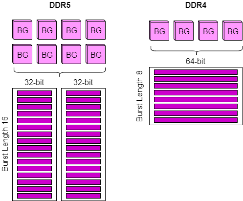
It’s similar with the 32-bit subchannels, except here we don’t just add more, we divide the existing 64-bit channel width in half. The reasoning for this is also relatively simply explained, more efficient control of the now increased number of bank groups and thus a faster processing of the commands, especially in situations where different applications cause work at the same time.
If the channel width is now halved, the maximum transmission rate per connection is theoretically also halved. This is where the burst length comes into play, i.e. how many bit sequences can be delivered in succession as a work package. While there were 8 of the 64-bit wide bursts in DDR4, this has simply been doubled to 16 in DDR5 to match the halved channel width of 32-bit. The result is logically the same 512 bits, only that now, due to the division into two channels, two of these connections can be used independently of each other.
Equally interesting is that by optimizing the channels, using multiple ranks through “nesting” or rank interleaving should no longer provide a performance boost. While dual-rank DDR4 was always faster for gaming in our tests as well, the same capacity is now available in single-rank DDR5 with equivalent optimizations. This in turn can be explained with the standardized memory density of 16 Gbit per chip, where at the start of DDR4 there were 4 and 8 Gbit variants.
8 memory chips with 16 Gbit each results in a module capacity of 16 GByte for a typical DDR5 module. This is also comparable with late DDR4 modules, e.g. based on 16 Gbit Rev B from Micron. However, there are some changes in the board layout aside from the memory IC’s. More about that in a moment, but before that I would like to take a look at the changes on the side of the Intel Alder Lake CPUs, which are supposed to get more performance out of the RAM, too.
Where previous 11th generation CPUs had only a single integrated memory controller or IMC, Intel has integrated a second one for the 12th generation. Bandwidth effectively remains the same with 2 channels of 64-bits, but multi-tasking should now be more efficient to implement. We could already confirm this in the tests of our CPU generation comparison with DDR4. Here, for example, Alder Lake manages to achieve almost 10 GB/s more throughput from the exact same RAM than Comet Lake in the AIDA64 Copy Test.
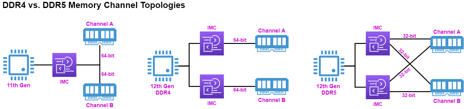
With DDR5 and the division of each channel into the two 32-bit subchannels, both IMCs now talk to both channels respectively and can thus distribute the work packets between the modules even more efficiently. If you now also consider that each channel can in turn contain up to 8 ranks, the performance potential of the new DDR5 standard becomes very evident. But now back to the memory modules and their construction.
Does the integrated ECC of DDR have an impact on performance or clock potential, possibly as a trade-off for latency?
On-Die ECC on the chip is extremely important for the scalability of the DRAM, because density and speed increase due to smaller wafer lithographies. We do not know if the on-die ECC functionality would have an impact on performance, if it wasn’t integrated.
On-Die ECC auf dem Chip ist für die Skalierbarkeit von DRAM von entscheidender Bedeutung, da Dichte und Geschwindigkeit durch niedrigere Wafer-Lithografien steigen. Uns ist nicht bekannt, ob die On-Die-ECC-Funktion die potenzielle Leistung beeinträchtigen würde, wenn diese Funktion nicht integriert wäre.
A further addition of DDR5 is the now on chip integrated on-die error correction code or OD-ECC. By using parity calculations the memory chips can detect errors during read or write operations that happen on the module and correct them on their own. However, by extension transfer errors that occur between CPU and RAM can’t be mitigated by this technology. For that the conventional ECC technologies will still be used in the server segment, as has been the case with DDR4. Additionally when overclocking DDR5 it could become quite important to check the actual performance gains. Because even if you can increase the frequency, when the memory chips are spending most of their time correcting errors, this could still result in a negative impact on overall performance.
A similar problem for example is seen on AMD Ryzen CPUs and their infinity fabric, where a higher clock might seem stable, but in reality cause lower performance due to the integrated error correction. Needless to say a corresponding DDR5 overclocking guide, including tipps on how to reliably measure the peformance, will follow from us as soon as more DDR5 modules will have made it to us. Speaking of the physical memory modules, let’s get back to them and their construction.


2 Antworten
Kommentar
Lade neue Kommentare
Mitglied
Alle Kommentare lesen unter igor´sLAB Community →