


Tear Down in the video
Since I now also run my own YouTube channel at many request, I also made a detailed video for this map for the Tear Down and also explained the most important measurements. The text here is of course much more detailed, but for a better understanding (also of the following pages) the video is certainly the right appetizer:
Board analysis
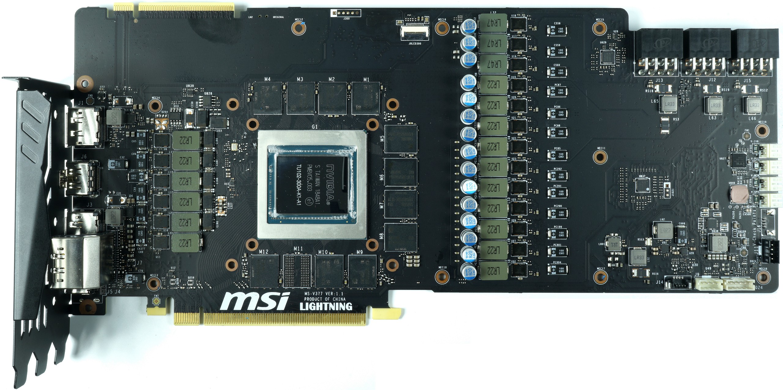
A very striking feature are the three thick 8-pin ATX power supply connections, although you can’t help but remember the LN2 BIOS. In contrast to the MSI GTX 2080 Ti Gaming X Trio, the fuses of the four 12-supply rails are also omitted, which would no longer work for the extreme OC anyway. And so each rail has at least one shunt, as well as a 330 mH coil for smoothing. It is a special feature that the GPU is completely powered only by the external connectors. But more on that later in the power consumption.
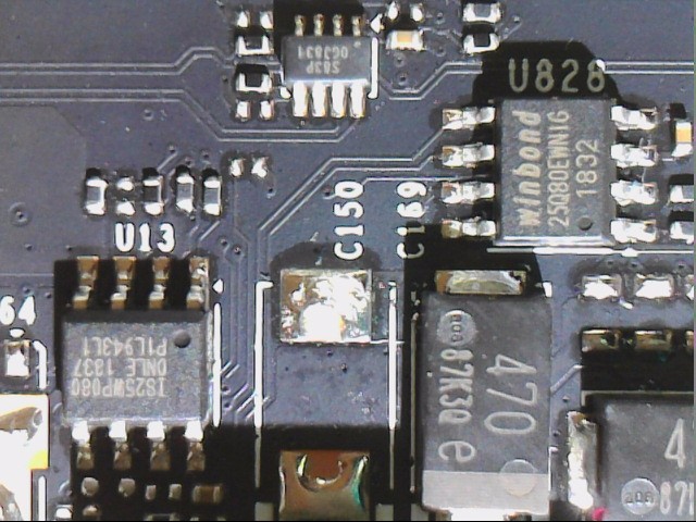
Despite the changed design, the board still looks quite tidy, although this is not really a feat with the sheer size of the board. In addition, however, the clip connector for the OLED display (top center) as well as the voltage taps for measurement purposes in the extreme OC (right center) were visibly implemented. In addition, two, instead of just one EEPROM for the BIOSe, are striking.
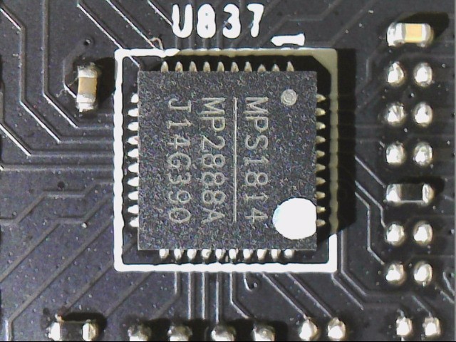
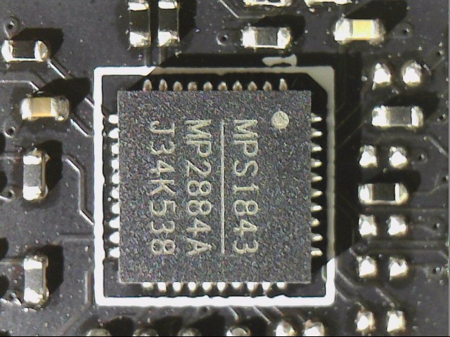
But let’s start with the power supply. Let’s start with phase splitting. An MP2888A from Monolithic Power Systems (MPS) takes on the task of the PWM controller, which is specifically designed to provide high-precision output voltage systems for the latest generation of GPUs. The integrated SMBus interface offers enough flexibility to optimize performance and efficiency and also to connect the right software
It also has programmable output voltage and active voltage positioning functions to adjust the output voltage depending on the load current, so that it is optimally positioned for a good load current transition. It also supports NVIDIA Open Voltage Regulator Type 4i+ with PWMVID function. The PWMVID input is buffered and filtered to create a very accurate reference voltage. The controller also supports new Smart Power Stage chips (PLCs). Appropriate PLC then provide very accurate information about e.g. currents (IMON) and temperatures (TMON).
One feature of the MP 2888A MP 2888A is the direct parallel connection of several voltage converter circuits without the usual doublers, since due to the necessary direct communication with the PLC no doubler chips can be used. We count a total of 16 voltage converter circuits for the GPU. However, since you rely on a neat 8-phase design, a total of eight real phases are double-connected. The three phases for memory are generated by a simpler MP 2884A (also from MPS) in true 3-phase mode.
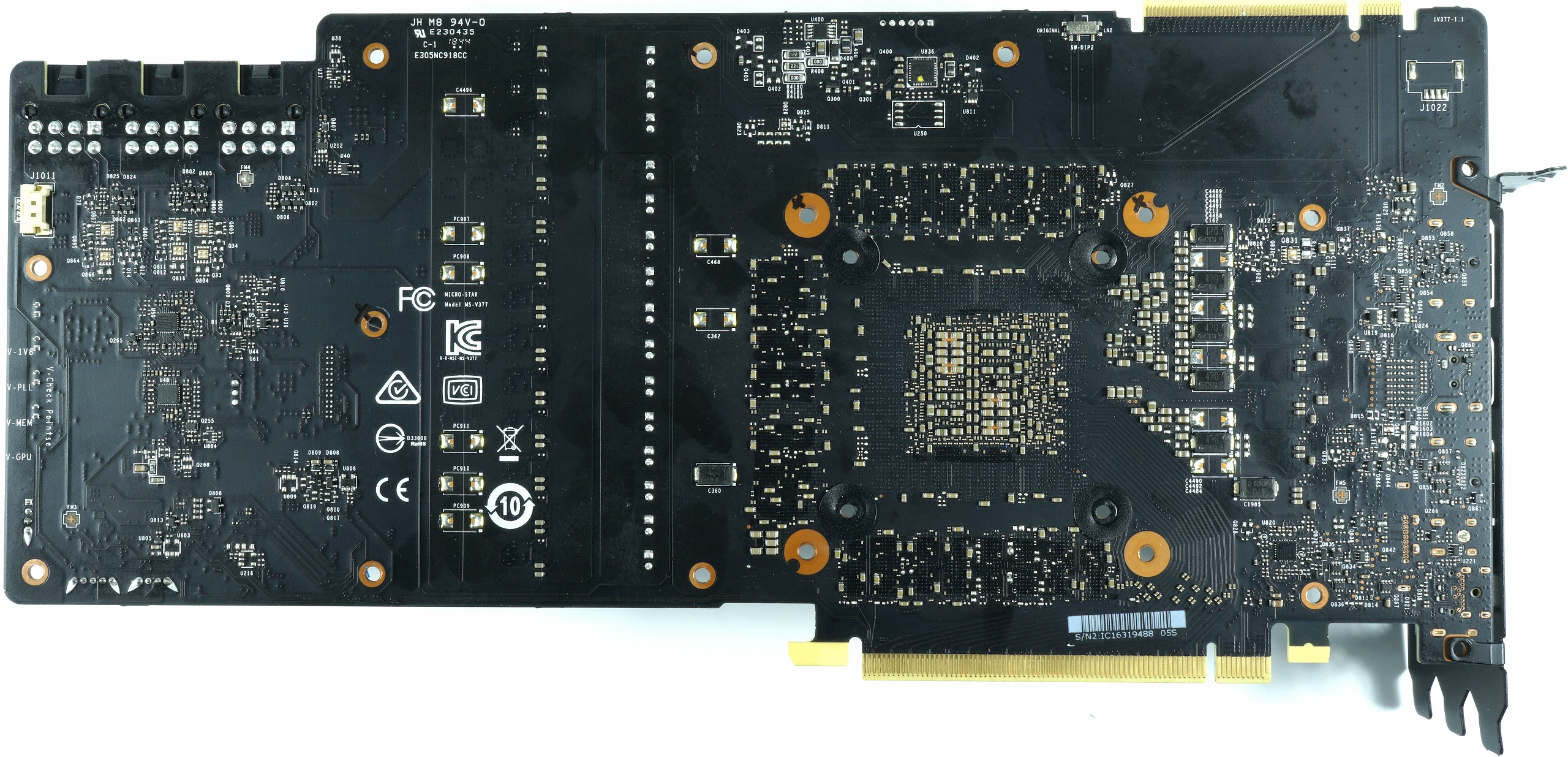
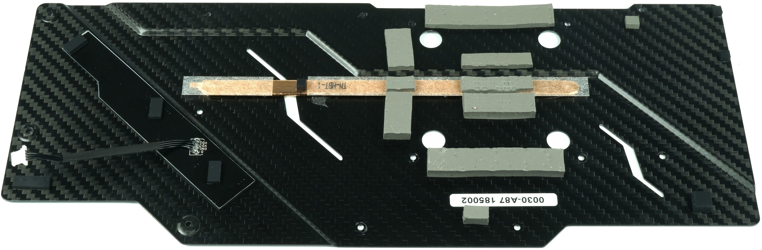
The back is free of secrets, except for two things. Once, it is the built-in ARM processor that is responsible for RGB and the OLED display. I recorded it again in the component collection below. And on the other hand, it is a small DIP switch that allows you to switch to the LN2 BIOS. This will play an important role later on.
If you would like to find out more details about this type of power supply and the improvements at Turing, please refer to our Investigative Article “Nvidia GeForce RTX 2080 Ti – Internal Details on Power Supply, Deviating Components and Where the Spikes which is always worth reading. There you will also learn more about the new Smart Power Stages, which replace the traditional, individual VRMs. The following table contains the most important components:
GPU Power Supply |
||
|---|---|---|
| PWM Controller | MP 2888A Monolithic Power Systems 8-phase/16 circles |
 |
| Gate Driver | not needed | |
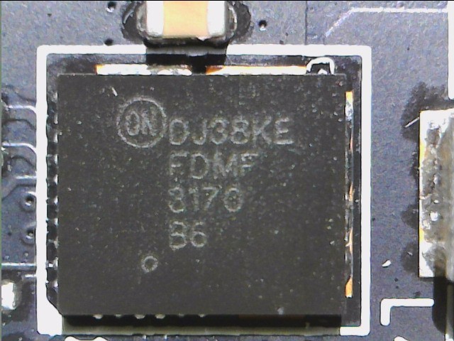
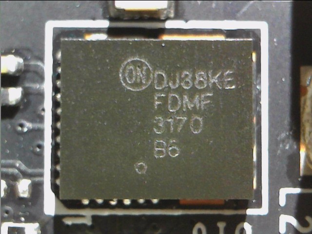
| Vrm | 16x FDMF 3170 (10 + 6) ON Semiconductor Smart Power Stage |
 |
| Coils | 16x Ferrite Choke 220 mH (10 + 6) |  |
Memory and power supply |
||
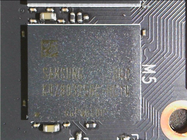
| Modules | K4Z803258C-HC14 Samsung 8x 8GB GDDR6 SGRAM Modules 2 Channels x 256 Meg x 16 I/O 2 Channels x 512 Meg x 8 I/O 14Gb/s |
 |
| PWM Controller | MP2884 Monolithic Power Systems 3 phases |
 |
| Vrm | FDMF 3170 ON Semiconductor Smart Power Stage |
 |
| Encapsulated Ferrite Choke 470nH |
 |
|
Other components |
||
| ARM Processor | 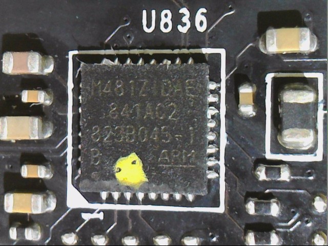 |
|
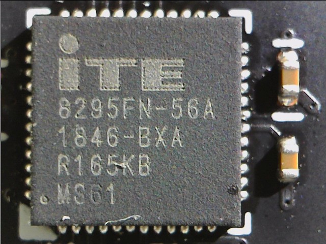
| Controller | 8915FN Ite Integrated embedded controller |
 |
| BIOS Switch | DIP Switch |  |
| Eeprom | 25WPo80 Eeprom Dual BIOS |
 |
| Shunts | 1x coil (smoothing) and shunt per 12V-rail (4) | 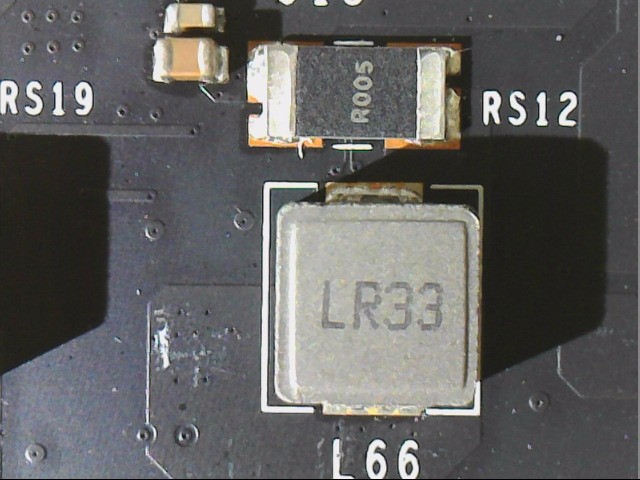 |
More details |
||
| Other Features |
– 3x 8-pin PCI-Express connectors for power supply – Filter coils in the entrance area |
|
Cooler and backplate in detail
The actual radiator structure alone weighs well over 1200 grams, including the cover and fans. Two thick 8 mm heatpipe and five 6 mm heatpipes then distribute the waste heat from the GPU heat sink to the cooling fins. This time, MSI uses a rather unusual fan arrangement with a smaller 8.5cm fan above the cooling frame, as well as two adjacent 9.5cm fans above the rest. We can see how well this works.
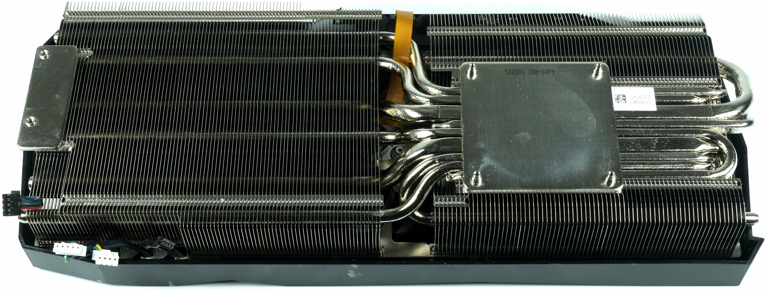
A large cooling frame permanently blown by the three fans additionally stabilizes the board and ensures cooling of the memory and voltage converters. MSI also relies on high-permeable formats, only 0.5 mm thick thermal guide pads. The range around the six individual voltage transformer circuits alone cannot fully show, as only the VRM is cooled here (picture below right side), while in the left, long row (10x GPU, 3x memory) also the coils and the input capacitors are cooled Be.
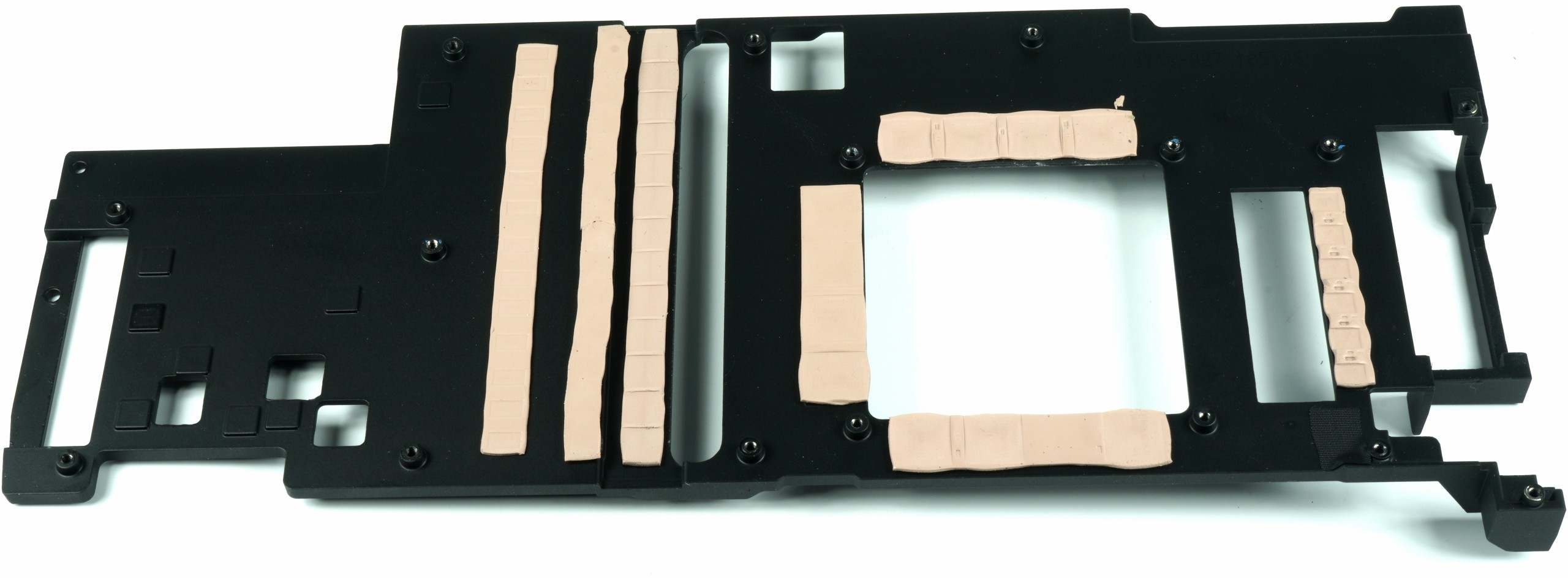
The lightweight, printed backplate made of carbon cools the storage indirectly via thermal guide pads, but the heat pipe could have been saved sooner. We will see later that the material of the backplate is a very bad heat conductor and that film between the heatpipe and the thermal guide pad also makes itself rather bad.
The cooling system briefly summarized in a tabular overview:
| Cooling system at a glance | |
|---|---|
| Type of cooler: | Air |
| Heatsink: | Nickel-plated heatsink, GPU |
| Cooling fins: | Aluminum, horizontal alignment related |
| Heatpipes | 2x 8mm, 5x 6 mm, nickel-plated |
| VRM cooling: | 16 (10 + 6) GPU VRM via built-in heat sink 3 Memory VRM via cooling frame |
| RAM cooling | via mounting frame |
| Fan: | 2x 9.5 cm fan, 14 rotor blades 1x 8.5 cm fan, 14 rotor blades semi-passive lyrised |
| Backplate | Carbon, heatpipe, thermal pads Conditional cooling function |


Kommentieren