


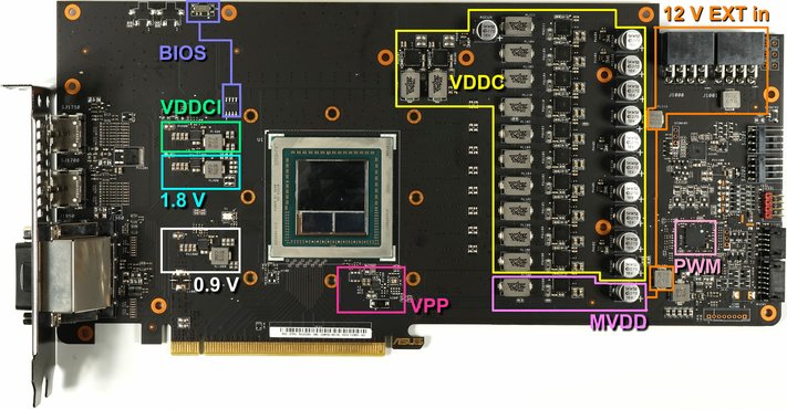
Board layout
Like Gigabyte and Sapphire, Asus is extremely different from AMD's reference layout, which should make the use of existing full-cover water coolers impossible. Asus relies on 6 phases with doubling, resulting in a total of 12 voltage converters for the VDDC and one phase for memory (MVDD). The production of the further auxiliary voltages is also shown in the diagram.
The positioning of two of the six voltage converters for the VDDC is interesting. Since there was no more space in the vertical row, it was simply placed to the left and must therefore cool it separately and differently. We will come back to that.
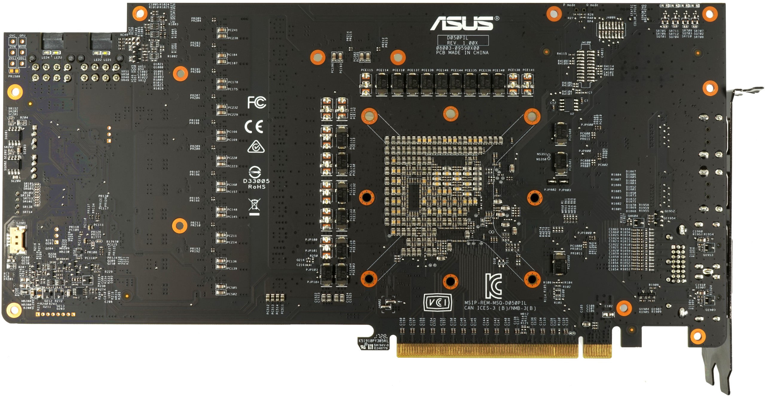
If you look at the back of the board, you can see that there are very few active components on this side and you would have had enough space to add a large thermal guide pad between PCB and backplate below the hot voltage converters. position.
Asus relies on a total of two external 8-pin sockets for power supply. Since the motherboard slot is about 25-27 watts maximum, these two connections must therefore handle the rest. We will see how much that is later.
GPU Power Supply (VDDC)
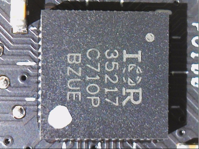
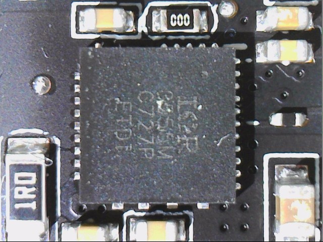
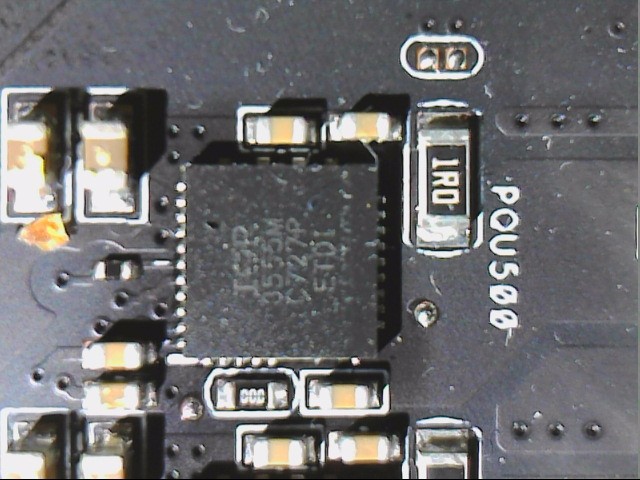
As with the reference design, the focus is on the IR35217 from International Rectifier, a dual output digital multi-phase controller that can provide both the six phases for the GPU and a wider phase for memory, which we are about to will come to speak. But back to the GPU and thus to what we see in the schema above as a VDDC block. We count 12 voltage transformer circuits, not six. However, since only six real phases are created, you double each of these phases in order to be able to divide the load into two converter circles per phase.
 |
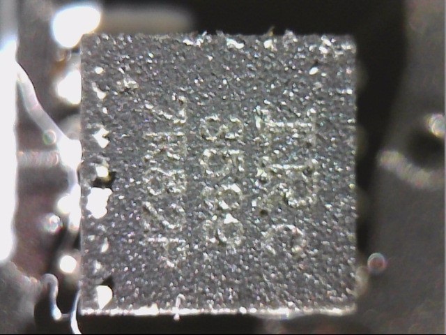 |
A total of six IR3599s from International Rectifier are used for this so-called doubling. The actual voltage conversion of each of the 12 converter circuits is carried out by an IR3555M, also from International Rectifier. These so-called PowIR Stage Chips combine the high and low side, as well as drivers and Schottky diode in a single, highly integrated circuit.
 |
 |
For the coils, Asus relies on your specially labeled SAP II ("Super Alloy Power") for both the VDDC and MVDD areas. These are in fairly neat, encapsulated and encapsulated ferrite core coils, which can also be equipped fully automatically.
Power supply of the memory (MVDD)
As mentioned briefly, the IR35217 also provides one phase for storage. One phase is sufficient for the card, as the memory is much more sufficient. As with the VDDC, we rely on an IR3555M from International Rectifier. The ALREADY mentioned SAP II ("Super Alloy Power") is used again for smoothing at the output.
 |
 |
Other voltage converters
The production of VDDCI is not a big item in terms of performance, but it is important. It is used for GPU-internal level transition between the GPU and memory signals, something like the voltage between the memory and the GPU core on the I/O bus. In addition, a constant source for 0.9 volts is generated. There is also a 1.8V source (TTL, GPU GPIO) on the front side. These three voltage converters are equipped almost identically and rely on an MPQ8633, a Synchronous Step-Down Converter from MPS.
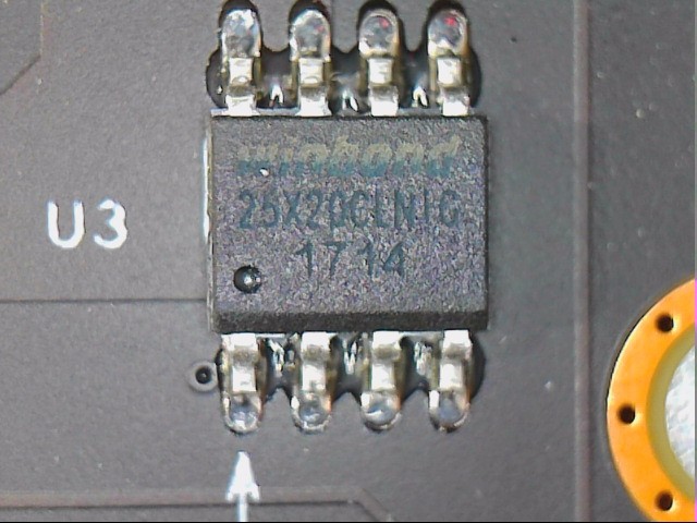
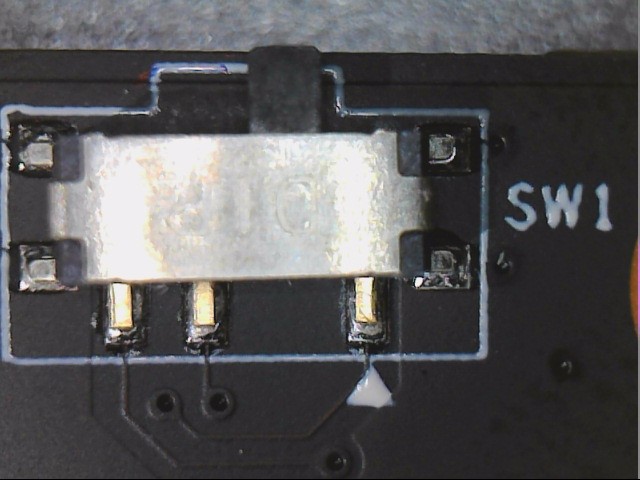
Below the GPU you can still find the APL5620 from Anpec for the VPP. This ultra-low dropout chip generates the very low voltage for the PLL range. Also striking is the dual BIOS chip 25X20xx, which is a double SPI flash chip. Asus has placed the right switch exactly where it can be found on the reference map.
 |
 |
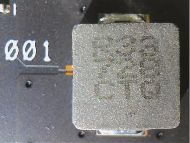
In the entrance area there is a ferrite core coil with 330 nH for input filtering, which helps to block the occurring load peaks including the incidental products of power supply. If you are looking for shunts in the entrance area as on the Nvidia cards, you won't find them, because Vega unfortunately does not support input-side current flow control.
 |
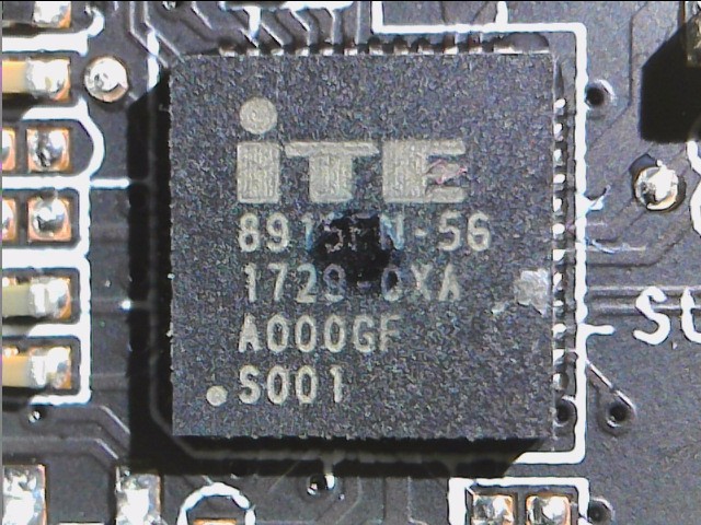 |
With the ITE 8915FN, Asus relies on a universal and programmable embedded controller that realizes fan control and RGB lighting effects. That would be the way we got through, because the rest is the usual standard.
- 1 - Einführung, Unboxing und technischen Daten
- 2 - Spannungsversorgung und detaillierte Platinenanalyse
- 3 - Gaming-Performance in WQHD (2560 x 1400 Pixel)
- 4 - Gaming-Performance in UHD (3840 x 2160 Pixel)
- 5 - Leistungsaufnahme im Detail
- 6 - Temperaturen, Taktraten, OC und Wärmebildanalyse
- 7 - Kühlerdetails und Geräuschentwicklung
- 8 - Zusammenfassung und Fazit


Kommentieren