


During the last days a lot of leaking has already taken place, nevertheless I have deliberately held back in order to be able to obtain more information in detail and above all to be able to verify it. I had to learn from my own information about Ampere often enough that most of the news of other media, based on it, were then unfortunately reproduced so superficially and technically without any expertise that the meaning was almost the opposite. And since there were and are always mistakes in the interpretation of the terms, I will now try to clarify some things about Navi21 XT and Navi21 XL and supplement them with my own (exclusive) information.
Power consumption: AMDs Graphics Power (“Socket Power”) is not equal to TGP (Nvidia)
Many of the news suggest, based on a leak by Patrick Schur, a power consumption of the Navi21 XT of 255 watts and the Navi 21 XL of 220 watts for the entire graphics card. This is not only wrong, but suggests an efficiency that unfortunately does not exist in this form. AMD calls the power consumption of the entire card TBP (Total/Typical Board Power) while NVIDIA calls the equivalent TGP (Total Graphics Power). So I can only advise those who write the daily news to go a little deeper into the subject matter they report on. Patrick was right, but from the sight of AMD. That’s a difference.
In AMD’s Graphics Power ONLY the supply voltages of the GPU for the GFX controller (VDDCR_GFX) and SOC controller (VDDCR_SOC) are included as the most important component, as well as the supply voltages for the memory as VDDMEM and VDDCI (controller and bus). AMD thus summarizes, in short, the pure GPU power consumption (“socket power”) and that of the memory. However, this value does not contain more than this! Furthermore, according to AMD’s Thermal Design Guide, as a TGP it refers only to the thermal load, i.e. the power dissipation to be cooled in these areas of the GPU and memory surface.
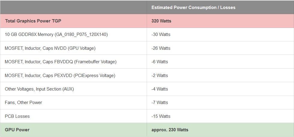
To get a fair comparison with NVIDIA now, you have to look at the whole thing in its entirety. I had already done the math for the GeForce RTX 3090 and was almost right on the watt. With the actual GPU power (according to NVIDIA’s Thermal Design Guide) of 228 watts for the GeForce RTX 3090, I ended up with only 2 watts difference. I transfer now the former calculation once to the GeForce RTX 3080 for better comparability:
Shall we do the same thing again for “Big Navi”? Since in this case the components like GPU and memory are already known (I’ll write something about memory a bit later), I’ll start this calculation from the other side. The whole thing is again strongly summarized and generalized (and also estimated), but it should be more or less the same. AMD should also use seven phases for VDDCR_GFX and one for VDDR_SOC in the voltage converter area, which doesn’t push the efficiency much, but is completely sufficient. Okay, that’s just a projection on my part, but it’s plausible.
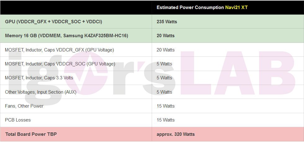
So we see that the actual power consumption of the Navi21 XT should be about the same level as that of the GeForce RTX 3080! You can’t reinvent physics and the Samsung process is not that much worse. Of course it’s worse, no question, otherwise NVIDIA wouldn’t have lost the efficiency advantage. And without the separation of the GPU voltage in NVVDD and MSVDD it would have gone even worse. But it is the way it is, and unfortunately even AMD cannot perform miracles.
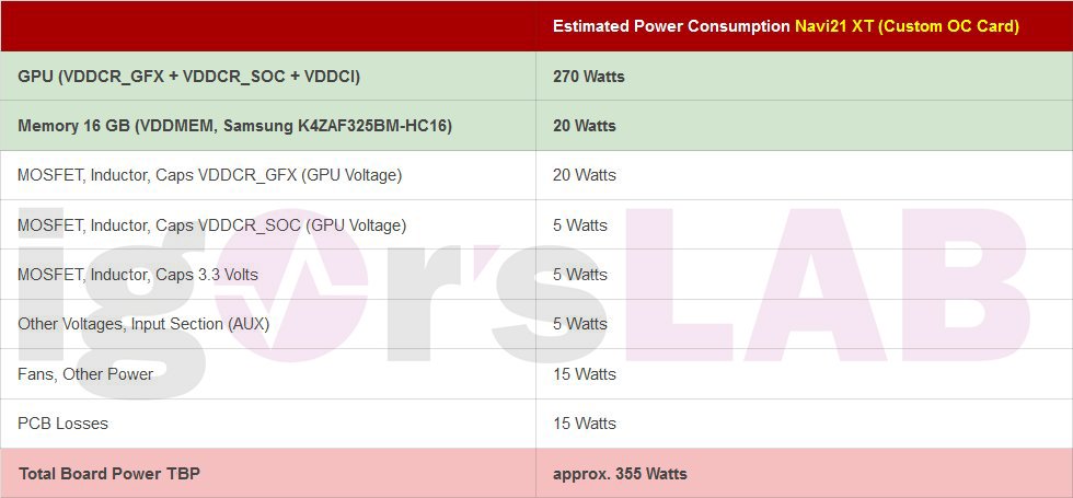
But what happens now with the board partner cards and the factory OC? Here, too, there are already clear indications as to where up to 290 watts of “graphics power” is allowed and will be seen. But then you’ll also be in areas that a GeForce RTX 3080 already covers during the cool season:
With the smaller version Navi 21 XL the calculation would look like this, because only memory with 14 Gbps is used and also the clock rate of the GPU is moch lower:
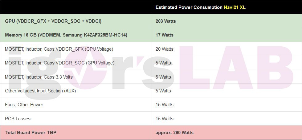
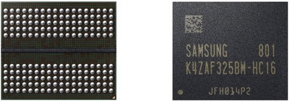
The used memory – Samsung is supposed to fix it with 16 Gbps
That the chip manufacturers give memory recommendations is nothing new, especially since AMD has often bundled the GPUs together with the memory as a package to the board partners, as is the case with NVIDIA. This time everything boils down to a pure (and emphatically formulated) recommendation, whereby the 16 gigabytes with 16 Gbps can probably only be realized with 8 modules in the form of the K4ZAF325BM-HC16 from Samsung at the moment. I will explain why you don’t dare to use double-sided boards in the section about the availability of the board partner cards.
It’s interesting that AMD only uses about 20 watts for the entire memory, which could well be an average value. However, experience with the 1 GB modules with 16 Gbps on NVIDIA cards shows that you should expect at least 1.5 watts per module, which would then amount to about 25 watts. The Navi21 XL as the smaller sister will also be slightly lower in power consumption with the lower clocked K4ZAF325BM-HC14.
And what about the overclocking margin and the undervolting?
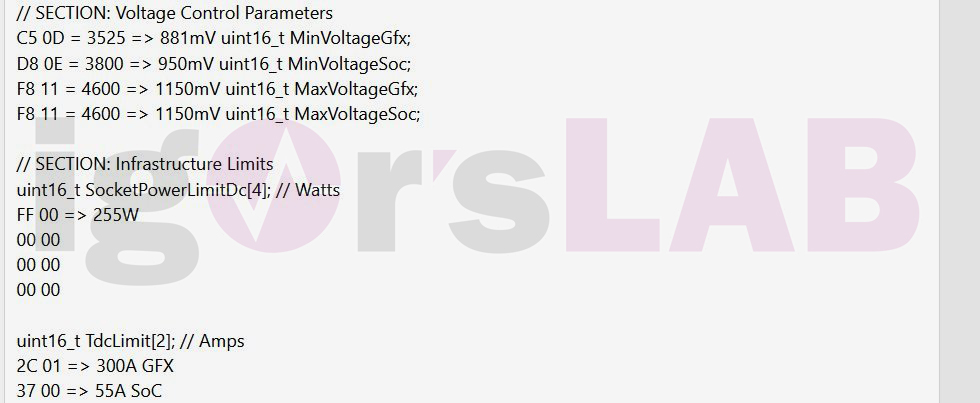
I also have exclusive news for you here, because the corresponding MorePowerTool will be available on our site to coincide with the launch. For certain reasons I will not spoil everything, because there are things like an NDA. But I can already give you a little appetizer. Should I? Okay, um…
Availability of board partner cards and driver games
And now we come to the most interesting point. If you are wondering what will happen to the boarding partner cards and when they will be available, you may be pleasantly surprised. Cards, such as a Sapphire Nitro or Asus Strix (which in turn should only be able to withstand MLCC), are expected to be delivered in smaller, technically feasible quantities as early as mid-November, while other manufacturers will (have to) allow themselves time until the end of November. If you are wondering now why all of a sudden this is happening so quickly and why so little information was available in advance, we would like to point out the rather simple adaptation process.
I was also led to believe that something completely new would come, which would need at least 2 months in advance. However, if you look at the circuit diagrams, an experienced observer may notice a lot of copy & paste to Navi10. However, since AMD’s board partners (AIB) can continue to rely on the proven board technology, do not need things like backdrill and also the voltage scheme remains more or less identical, there is no need to reinvent the wheel here. NVIDIA’s effort with the highly clocked memory and split supply voltages is thus eliminated, which almost degrades an adaptation to a loosening up exercise. It can be assumed that the circuit boards for the Navi 21 XT and XL will look very similar to those of the Navi 10. Anything else would be astonishing.
And there is a delicate parallel to NVIDIA, namely the drivers for the evaluation boards (we are now in the EVT phase), currently a driver called Beta8. Also AMD has completely limited the graphics performance to avoid annoying leaks. Corresponding reports that board partners had complained about insufficient performance were answered exactly the same way by AMD. So the AIB don’t know (like NVIDIA’s AIC in September) what they are actually producing. Not bad either.


Kommentieren