


Infinity Fabric and the bridge between all parts
AMD's "Infinity Fabric" is a flexible and coherent interface/bus system that enables AMD to quickly and efficiently integrate a sophisticated IP portfolio into a coherent die. All these composite parts can use infinity fabric to create data between the individual CCXs, system memory, and other controllers (e.g. memory, I/O, PCIe) that are on the package.
The Infinity Fabric also gives the "Zen" architecture the command and control options needed for real-time estimates and adjustments of core voltage, temperature, power consumption, clock frequency and more. This command and control functionality is also critical to AMD's SenseMI technology, which we've already discussed on the previous page.
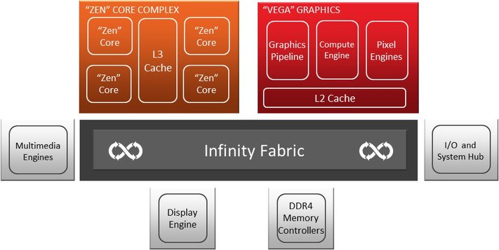
With the graphics unit based on the "Vega" architecture and also integrated with the APU, AMD is offering a new generation of GPUs that will have received over 200 changes and improvements in the redesign of the architecture. Even if in the end it probably boils down to a kind of new GCN generation: AMD repeatedly emphasizes that it is a completely new solution.
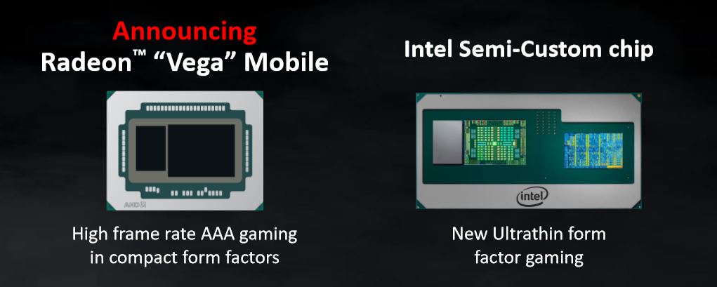
The implementation of the mobile Vega offshoots can be found not only in the two APUs presented today, but also in Intel's semi-custom chips, which will surely be launched soon, but where a completely different approach has been adopted. It will be exciting to see how both solutions will beat each other in the near future and where the respective advantages and disadvantages can be found. Without a direct comparison, it is difficult to predict anything.
New programmable geometry pipeline
Let's just remember: The first HawaiiGPU on the Radeon R9 290 X brought some notable improvements compared to the Tahiti GPU on the Radeon HD 7970. One of them concerned an improved front end with now four instead of two geometry units, each of which each had a Geometry assembler, a Vertex assembler, and a tessellation unit.
The subsequent Fiji GPU as Radeon R9 Fury X then again relied on this already known hawaiian configuration, but brought with it some other innovations – for example, a significantly increased tessellation performance. Currently, the Ellesmere GPU (Radeon RX 480) uses a new handful of techniques to use the same constellation with the four geometry units through various filter algorithms or discarding unnecessary polygons to provide a performance benefit.
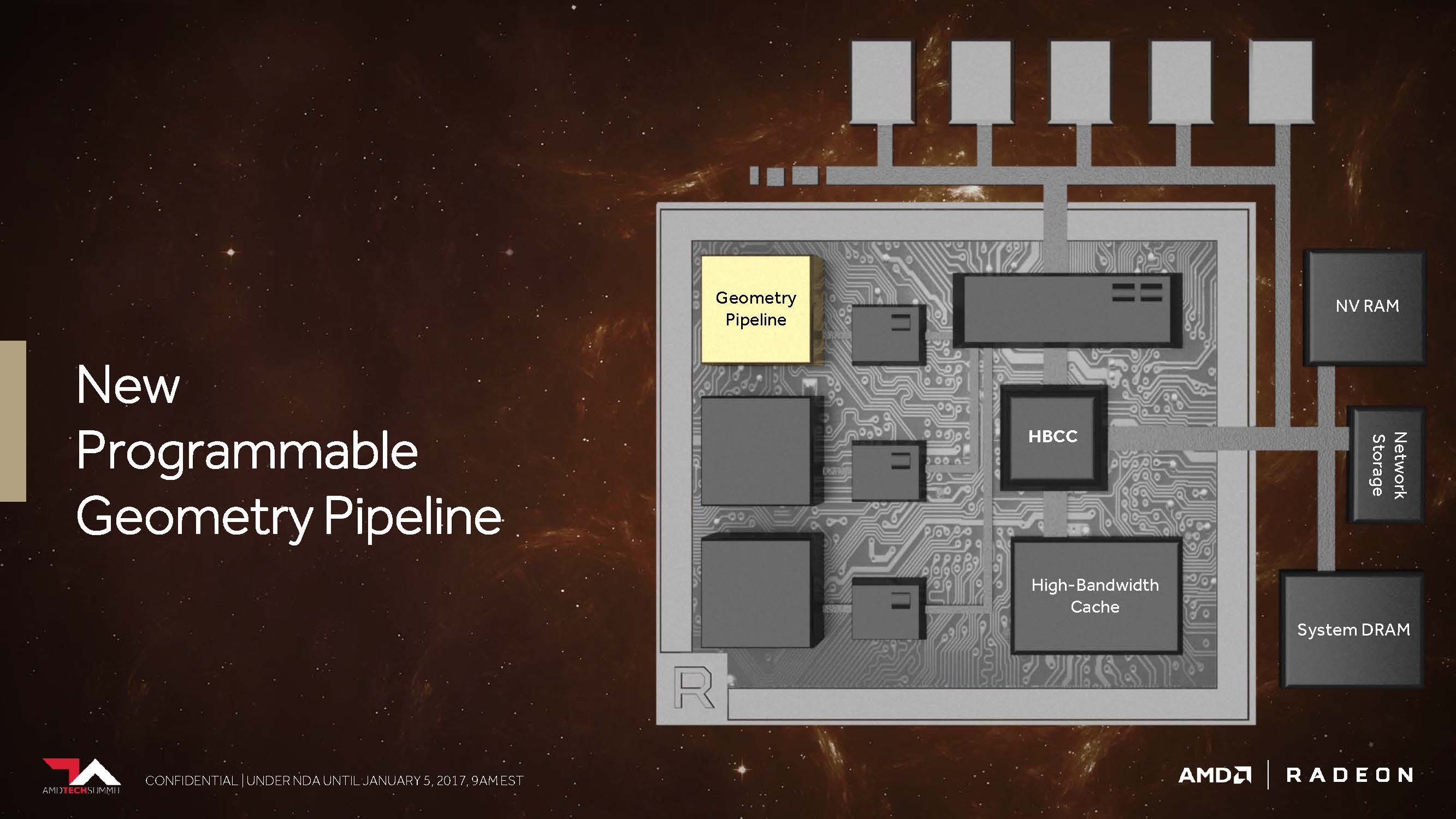
AMD promised us last year that Vega would now be able to work up to 11 polygons at the top instead of the maximum four polygons per cycle, which is up to 2.75 times that. This is supposed to be the result of what AMD has inserted into the geometry pipeline as the New Primitive Shader Stage. According to AMD (Tech Day in Sonoma, 2017), a flexible shader array is used to process the resulting polygons instead of the hardware-anchored but inflexible functions.
This can best be compared with the functionality of a compute shader for processing the geometry tasks – easy and programmable, and equipped with the ability to discard unnecessary polygons at a high rate. Of course, this shader functionality also contains much of what DirectX offers with its vertex, envelope, domain, and geometry shader levels, but you want to be more flexible in the order and priority of the actual processing.
After all the discussions that have occurred since the Vega launch, AMD has re-specified the statements on this option and also provided an amended scheme.
Vega's new primitive shader support makes it possible to combine parts of the geometry processing pipeline and replace them with a new, highly efficient shader type (picture below). These flexible, universally applicable shaders can also be implemented and then enable more than four times the maximum primitive cull rate per clock cycle.
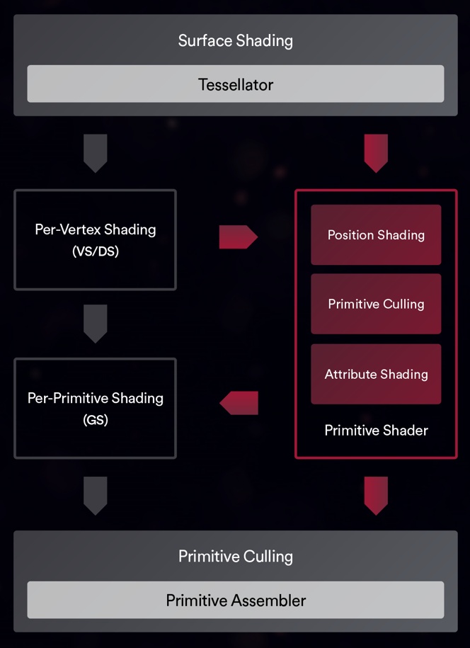
The approach is logical, because in a typical scene about half of the geometry is discarded by various techniques such as Frustum Culling, Backface Culling and Small Primitive Culling. The faster these primitives are discarded, the faster the graphics processor can start rendering the visible geometry.
In addition, traditional geometry pipelines discard primitives only after vertex processing is complete, which can lead to unnecessary waste of compute resources and bottlenecks in storing a large amount of unnecessary attributes. Primitive shaders, on the other hand, allow for early removal to conserve these resources.
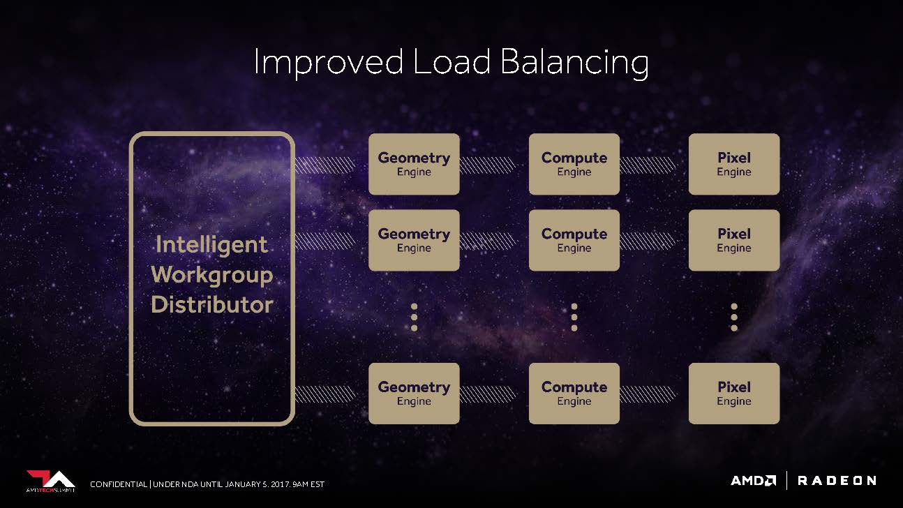
The frontend also benefits from an improved "Workgroup Distributor", which should be able to ensure the best possible load balancing around the now programmable hardware.
The Vega-NCU (Next-Generation Compute Unit)
TODAY, GPUs often use more mathematical precision than they would have needed for the calculations they are performing. Years ago, GPU hardware was optimized exclusively for processing the 32-bit floating-point operations that had become the standard for 3D graphics. However, as rendering engines have become more sophisticated and graphics processor applications go beyond graphics processing, the value of data types beyond FP32 has increased.
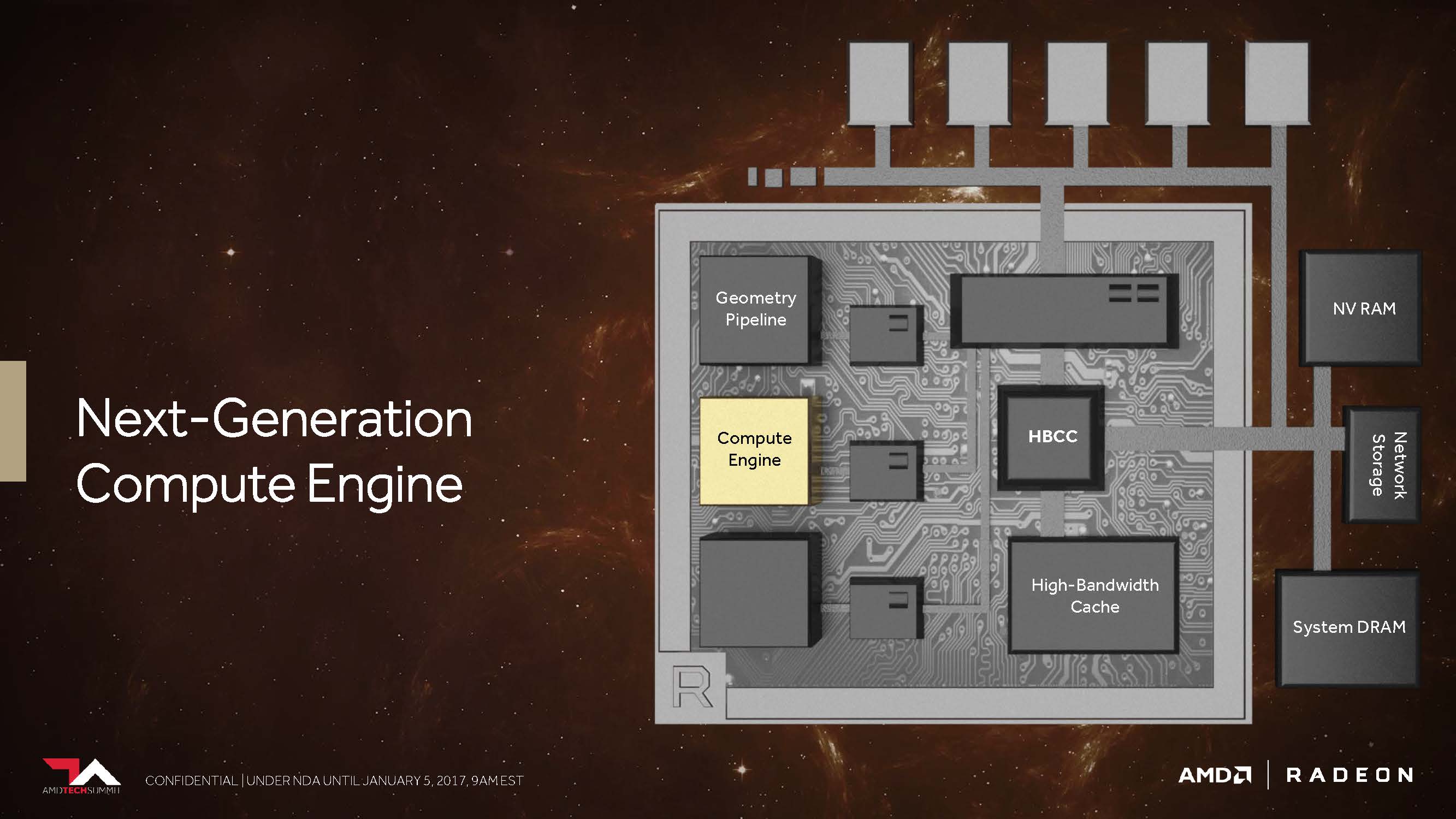
But what does Vega have, for example, what Polaris hasn't had it yet? The CU block with its 64 IEEE 754-2008 compatible shaders remains as such – only that AMD now calls it NCU (Next-Generation Compute Unit), which also includes support for new data types. Logically, these 64 shaders, together with your maximum power of two floating-point operations per cycle, result in a maximum of 128 32-bit operations per cycle.
The programmable computing units, which form the heart of the "Vega" graphics processors, have been provided with an additional function called Rapid Packed Math. Enhanced support for 16-bit packed content doubles floating-point and integer rates compared to the known 32-bit operations. It also halves the register space and the data flow required to handle a certain number of operations. The new command set includes a rich mix of 16-bit floating-point and integer commands, including FMA, MUL, ADD, MIN/MAX/MED, bit shifts, packing operations, and more.
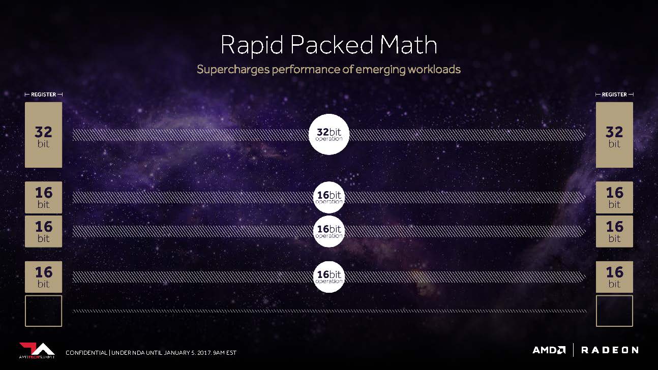
In detail, this means that if you use F16-packed calculations, you can already perform up to 256 16-bit operations per cycle. AMD concludes that, under optimal conditions, it could even be up to 512 8-bit operations per cycle cycle. The impetus for this flexibility may have come from the console world. After all, we know that Sony's PlayStation 4 Pro can achieve up to 8.4 TFLOPS in FP16 performance, twice its performance in 32-bit operations.
For applications that can take advantage of this capability, Rapid Packed Math can significantly improve computational throughput and energy efficiency (Figure 8). In the case of specialized applications such as machine learning and training, video processing and VR, 16-bit data types are an obvious solution, but there are also benefits for more traditional rendering operations.
Modern games, for example, use a variety of data types in addition to the FP32 standard. Normal/direction vectors, light values, HDR color values, and glare factors are just a few examples of using 16-bit operations.
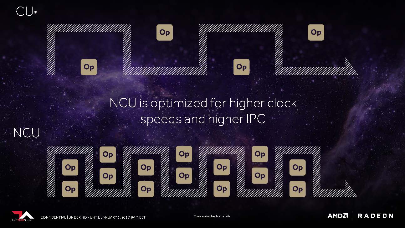
In the end, it may even be both to poach in areas outside of Nvidia's current market presence. In both cases, new consoles, entire data centers and, of course, PC gamers as well as semi-professional users can benefit to the same extent. In addition to the fact that the NCUs have also been optimized for higher clock rates, it also relies on larger instruction buffers in order to be able to use the computing units as well as possible over the entire time. And what the dedicated desktop graphics card is right for can only be cheap for built-in graphics in the APU.
Next-Generation Pixel Engine
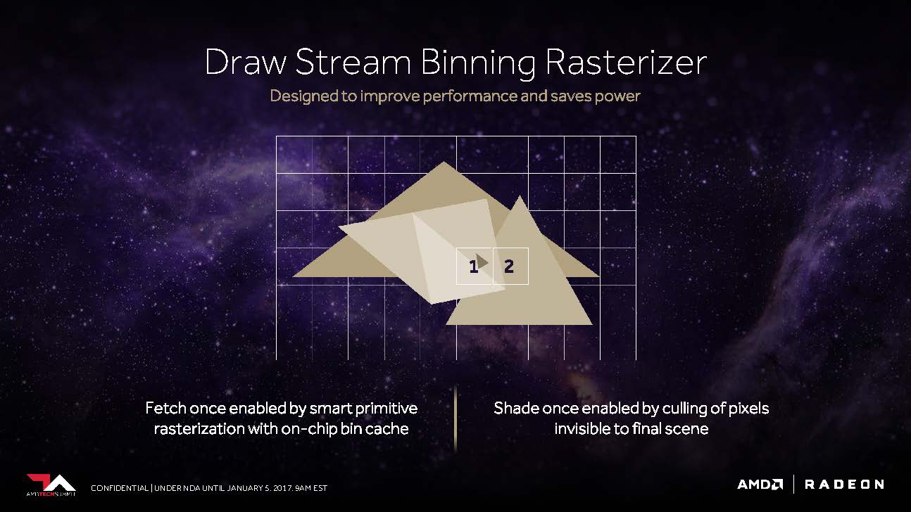
Let's move on to what AMD calls the "Draw Stream Binning Rasterizer" and which, as a complement to the traditional ROP, should be able to increase performance while also saving energy.
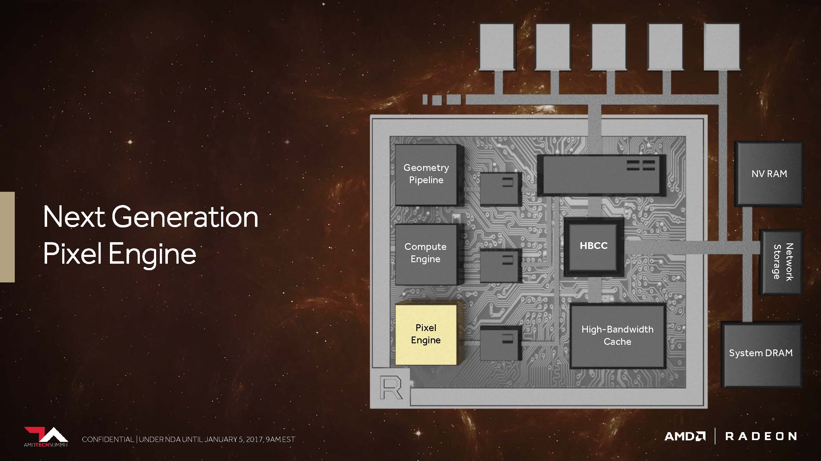
Thus, a special cache on the chip should allow the rasterizer to edit the data for intersecting polygons only once and oothe all those pixels that would not be visible in the finished scene anyway.
The second point is that AMD has changed its cache hierarchy in general and fundamentally so that the rendering backends are now directly connected to the L2 cache.
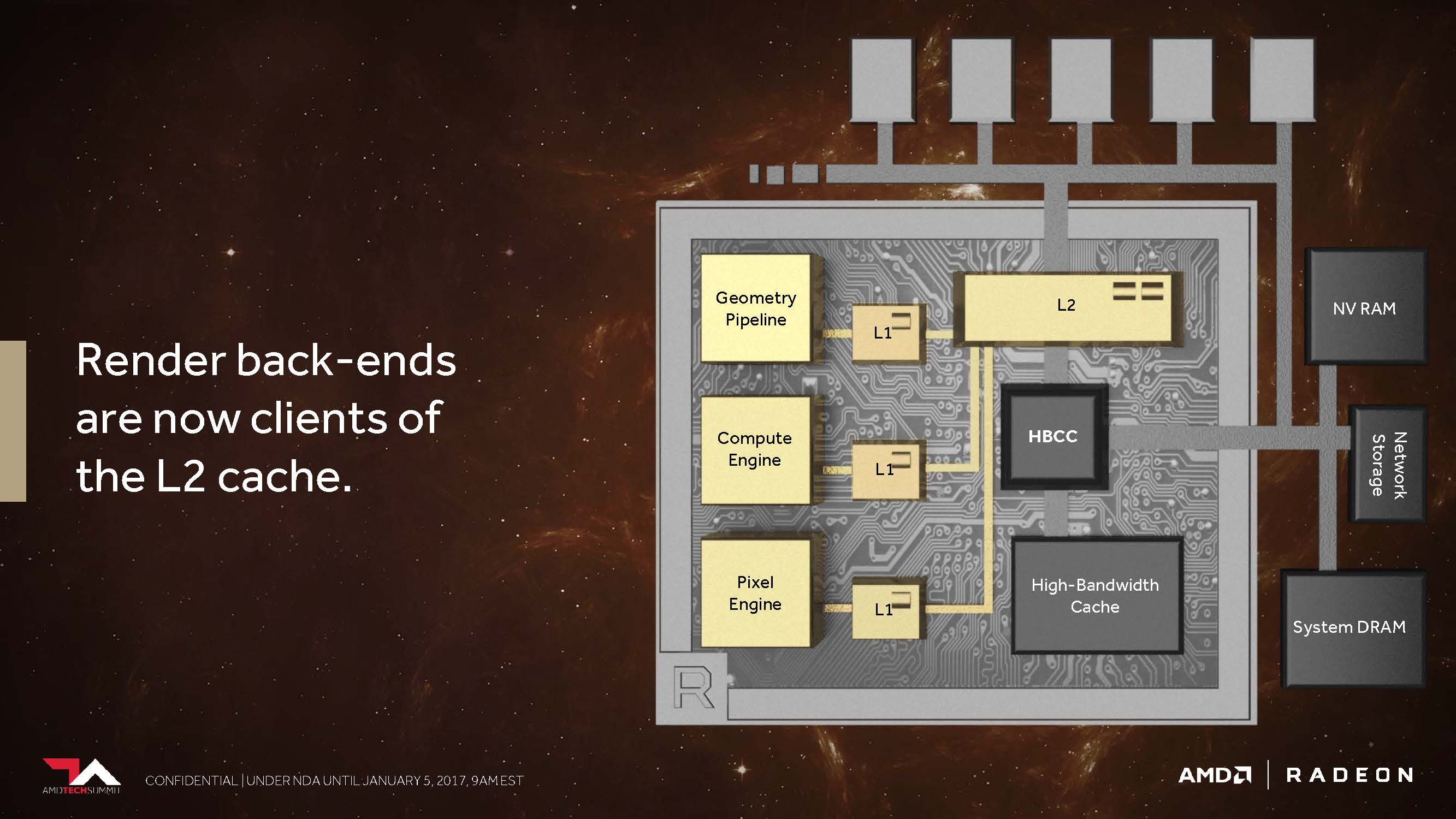
In the pre-Vega architectures, AMD did not have proper memory access for non-coherent pixels or textures that would have allowed each pipeline stage to synchronize them over a shared point. For example, a texture rendered as a result of a scene for later use was sent all the way back to the graphics memory outside the graphics chip before it could be recalled. AMD now handles all of this with the coherent access, which , as AMD says, should offer an enormous increase in performance whenever, for example, Deffered Shading is used.
- 1 - Einführung und Testsystem
- 2 - Ryzen als Basis, aber mit Verbesserungen
- 3 - Kernschmelze von Zen und Vega für die Grafik
- 4 - Gaming: Vorwort und 3DMark
- 5 - Gaming: Battlefield 1
- 6 - Gaming: Civilization VI
- 7 - Gaming: Grand Theft Auto V
- 8 - Gaming: Dota
- 9 - Gaming: Far Cry Primals
- 10 - Gaming: The Witcher 3
- 11 - Anwendungs- und Office-Benchmarks
- 12 - Zusammenfassung und Fazit


Kommentieren