


Zen becomes Ryzen
But let's go back to our little introductory course, which we had already started on the first page. It all started, of course, with the core as such. Five years ago, AMD started the development of the Zen core, creating (finally) the first new architecture since Bulldozer. AT the same time, AMD's goal was to switch from outdated 28 nm process technology to Globalfoundrie's new 14 nm FinFET process, which also allows for improved density and performance with comparable energy uptake.
AMD also set itself the ambitious goal of increasing IPC performance (Instructions Per Clock) by a whopping 40 percent compared to Excavator by a series of architectural design decisions that are expected to significantly increase performance. Once again, AMD has simultaneously implemented a new microarchitecture and a new lithography process, which was quite a mammoth project.
 Ryzen CPU Die-Sot
The Zen core acts as a fundamental building block for Ryzen and all future AMD CPUs or APUs, will cover applications from notebooks to supercomputers. Ryzen processors integrate two 4-core Zen CCX' (CPU Complex) with a total of 4.8 billion transistors, while the current APUs only integrate one each. AMD's new Infinity Fabric, an optimized version of HyperTransport, now connects all relevant areas. So these are basically two quad-core CPUs that communicate with each other via an on-die connection, which also connects the Northbridge and the PCIe lanes.
"Raven Ridge" essentially replaces the second CCX with a graphics engine with Vega architecture. Thus, the whole is divided into a CCX, the Vega GGPU and the Uncore. The Uncore includes an Infinity Controller, Infinity Fabric and I/O and System Hub. While the "Zeppelin" which consists of 4.8 billion transistors on an area of 213 mm2, the "Raven Ridge" has 4.94 billion transistors and measures 209.8 mm2.
 Ryzen APU Die-Shot
Unlike previous Ryzen products, as mentioned on the previous page, all four execution cores are in a single CCX (orange block on the left side of the image above). This means that an application running on multiple cores does not have to traverse Infinity Fabric to communicate with other cores and the cache. From previous tests, we know that working with a number of "remote" cores (and the cache) in the Infinity Fabric improves performance in latency-sensitive applications, such as playing, negatively affecting. Raven Ridge's Single CCX should do better in such situations.
We have marked the four-core CCXes with the green box. Similar to AMD's "Zeppelin" which contains the center of a "Raven Ridge" CCX vertical rows with L3 cache, but in total only 4 MB instead of 8 MB. This means that it is a purely architectural design choice to save space.
The orange block in the upper left corner of Raven Ridge contains the interconnect and control units, as with Zeppelin. But the DDR4 memory controllers and the platform I/O circuits at the edges are located in different places. Work has definitely been done to optimize the layout. And although the cores themselves appear identical, the CCX design is new.
Raven Ridge processors use Infinity Fabric to connect the CPU cores and the On-Die Vega CUs (the blue block on the right). But in the end it is only a kind of protocol. This means that a number of physical connections can be traversed, such as interposer, traces or internal PCIe lanes. One might suspect that this protocol works on an internal PCIe bus and that the graphics engine also consumes some of the available connectivity, which is why Raven Ridge's externally accessible lanes have been reduced to eight. It's also possible that the drop from 16 to eight lanes was simply another design choice, as was the reduced L3 cache.
We have also made some of our own measurements on this topic:


AMD has also donated SMT (Simultaneous Multi-Threading) to the Zen core, providing every physical one with a virtual core – known in Intel's parlance as hyper-threading. Ryzen was AMD's first SMT-enabled processor, and the Ryzen 5 2400G also offers this feature.
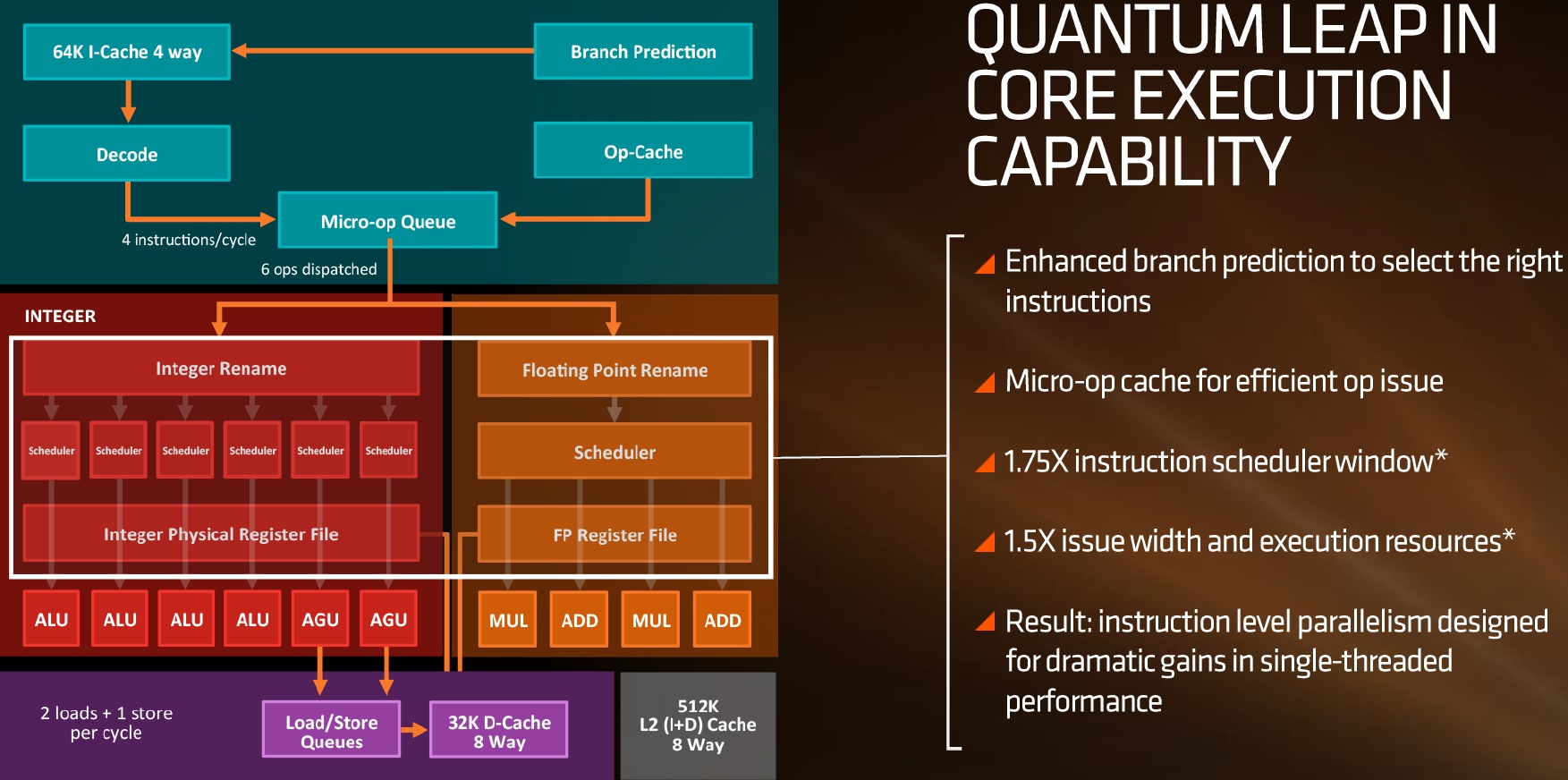
In addition to many other architectural enhancements, the company has also integrated a micro-op cache to bypass the L1 and L2 caches for commonly used microoperations. AMD also wants to improve the Branch Prediction Engine, increase the Instruction Scheduler window by 1.75 times, and increase L1 and L2 cache performance nearly 2 x.
Pure Power
AMD's SenseMI suite actually consists of five key technologies that allow AMD's Ryzen processors to adjust performance and power consumption parameters in real time. Let's start with what AMD likes to promote as "Pure Power." AMD's Zen architecture uses an array of 1000 sensitive sensors to accurately measure up to 1mAh, 1mV and 1C. AMD's Pure Power function monitors temperature and voltage, allowing real-time parameter adjustments based on decisions made by learning algorithms.
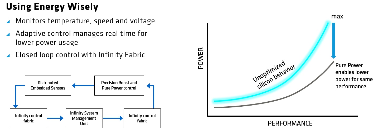
These sensors feed the Infinity System Management Unit with telemetry data at 1000 ms intervals via the Infinity Factory Loop. The Management Engine then analyzes the data and issues commands over the fabric to adjust voltage and clock speed for optimal performance. AMD also noted that this should help manage speculative cache features and AI-based branch prediction.
Each piece of silicon is unique in detail, and according to AMD, its algorithms are designed to allow the processor to optimize itself in the best possible way based on its unique features. At this point, however, it should be noted that most current processors use a similar technique to dynamically adjust their power consumption.
Our following picture gallery provides an accurate overview of the topic of power supply and the division between CPU and GPU:


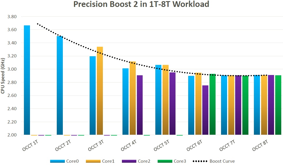
Precision Boost 2
Precision Boost, as a telemetry-capable DVFS technology, optimally adjusts the power consumption performance curve to the respective operating conditions – similar to Intel's Turbo Boost – using information generated by the Pure Power feature. Precision Boost algorithms adjust clock and voltage in real time in a granular way – but where Intel adjusts the clock clock in 100 MHz increments, AMD now works with 25 MHz steps.
Ryzen desktop processors use this boost algorithm in two discrete states: three or more CPU cores ("All-Core Boost") or "All-Core Boost". Two or fewer CPU cores ("Two-Core Boost"). Only – if you e.g. three cores is needed, then this somewhat too simple logic recreates all cores equally ("all-core boost"), which is not really optimal and is also an unnecessary waste of resources. In addition, there is actually no full workload yet, so there is no imminent electrical, thermal or usage limit that would virtually rule out a further increase in clock rate. This is where version2 used in the APUs starts.
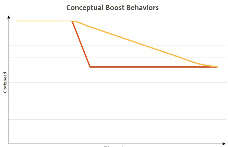
The remaining thermal, electrical and usage-related headroom can be safely converted into higher clock rates in order to make better use of the remaining reserves. Precision Boost 2 thus also relies on the 25 MHz steps of its predecessor, but at the same time also uses an algorithm that intelligently tracks the highest possible frequency until one of the above limits reaches or simply achieves the maximum frequency target (whichever occurs first). This applies to any number of threads and in real time, but without any arbitrary limitations. Precision Boost 2 is thus a real development, as the two graphics show.
Neural Net Prediction & Smart Prefetch
According to AMD, its Neural Net Prediction consists of a neural network that learns from the behavior of applications, so that CPU instructions are available before they are needed.
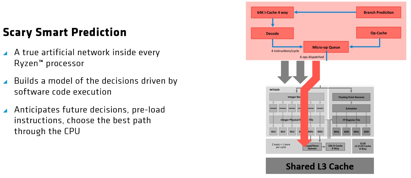
Smart Prefetch, on the other hand, selects the best data path through the CPU and loads data into cache memory for faster execution before it is needed.
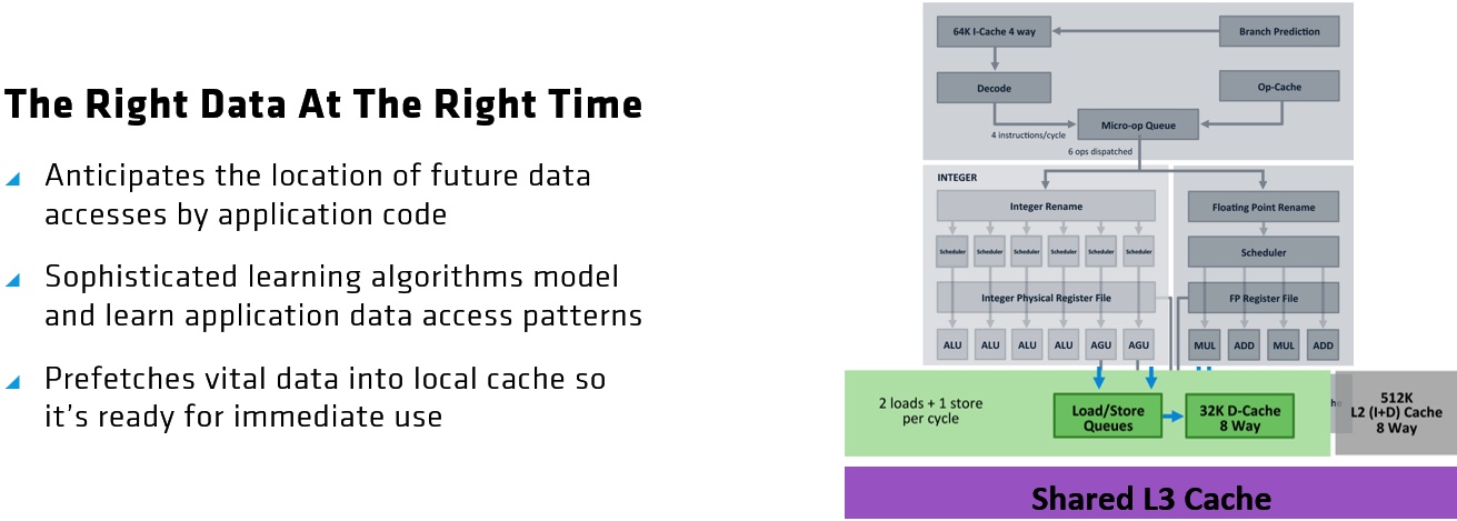
Both features are, of course, marketing labels for AMD's Perceptron Branch Predictor. We've known this term since AMD's Jaguar cores, and we've just further optimized this jump prediction for the Zen microarchitecture. But it is ultimately nothing more than a common technology. However, aside from the usual marketing buzzwords, the Zen microarchitecture offers significant innovations and benefits compared to previous AMD architectures.
- 1 - Einführung und Testsystem
- 2 - Ryzen als Basis, aber mit Verbesserungen
- 3 - Kernschmelze von Zen und Vega für die Grafik
- 4 - Gaming: Vorwort und 3DMark
- 5 - Gaming: Battlefield 1
- 6 - Gaming: Civilization VI
- 7 - Gaming: Grand Theft Auto V
- 8 - Gaming: Dota
- 9 - Gaming: Far Cry Primals
- 10 - Gaming: The Witcher 3
- 11 - Anwendungs- und Office-Benchmarks
- 12 - Zusammenfassung und Fazit


Kommentieren